
A conductive ink with circuit etching performance and its preparation method and application

A conductive ink and etching technology, applied in the direction of ink, application, printed circuit manufacturing, etc., can solve the problems of high equipment cost and energy consumption, low production efficiency, large water consumption, etc., achieve good conductivity, meet market demand, The effect of strong adhesion

Active Publication Date: 2020-10-16
NANXIONG MATERIAL PRODION BASE OF CHINESE ACADEMY OF SCI GUANGZHOU CHEM +2
View PDF2 Cites 0 Cited by
  • Summary
  • Abstract
  • Description
  • Claims
  • Application Information

AI Technical Summary

Problems solved by technology

The traditional process of manufacturing printed circuit boards includes pressing the metal film on the surface of the substrate, and then forming a photoresist layer on the surface of the metal film by spin coating, and then exposing, developing, and etching with a mask, and then drilling. , pressing and electroplating and many other steps, and many tests and repairs are required to complete the whole process, which will affect the quality of the product
The traditional method of manufacturing printed circuit boards is not only complicated, but also requires equipment such as ultraviolet curing, etching, alkali cleaning, water washing, and air knife. Cause environmental pollution, process conditions are difficult to control, production efficiency is low, and market demand cannot be met

Method used


Image

  • A conductive ink with circuit etching performance and its preparation method and application
  • A conductive ink with circuit etching performance and its preparation method and application
  • A conductive ink with circuit etching performance and its preparation method and application

Examples


Embodiment 1

[0085] (1) Preparation of conductive ink: Calculated by mass parts, 50 parts of metallic silver powder (flake silver powder with a particle size of 1-10 μm), 15 parts of high acid value matrix resin (high acid value epoxy resin EB), 15 parts of light 1 part of initiator benzoin dimethyl ether (DMPA), 0.5 part of defoamer polyoxyethylene polyoxypropylene pentaerythritol ether, 0.5 part of acrylate leveling agent dissolved in 33 parts of organic solvent acetone, fully mixed by ultrasonic, ultrasonic power is 100W, the ultrasonic time is 30min, and the conductive ink is obtained.

[0086] (2) Coating conductive ink coating: apply the conductive ink obtained in step (1) on the glass sheet by the coating bar coating method, and then let it stand to dry under natural conditions or dry at 80°C in an oven to obtain conductive ink. ink layer.

[0087] (3) Light curing: Cover the conductive ink layer obtained in step (2) with a mask plate with a specific circuit, and then cure it under...

Embodiment 2

[0091] (1) Preparation of conductive ink: Calculated by mass parts, 58 parts of metallic silver powder (flaky silver powder with a particle size of 1-10 μm), 12 parts of high acid value matrix resin (EB), photoinitiator benzophenone (BP) 1.5 parts, defoaming agent polyoxypropylene glyceryl ether 0.5 parts, organosiloxane leveling agent 1 part dissolved in 27 parts of organic solvent acetone, fully mixed by ultrasonic, ultrasonic power 100W, ultrasonic time 30min, obtained conductive ink.

[0092] (2) Coating conductive ink coating: apply the conductive ink obtained in step (1) on the glass sheet by the coating bar coating method, and then let it stand to dry under natural conditions or dry at 80°C in an oven to obtain conductive ink. ink layer.

[0093] (3) Photocuring: Cover the conductive ink layer obtained in step (2) with a mask plate with a specific circuit, and then cure it under the condition of UV irradiation for 700s, the power of the UV lamp is 1000W, and the irradi...

Embodiment 3

[0097] (1) Preparation of conductive ink: Calculated by mass parts, 64 parts of metallic silver powder (flaky silver powder with a particle size of 1-10 μm), 16 parts of high acid value matrix resin (EB), photoinitiator 1-hydroxyl ring 1.5 parts of hexyl phenyl ketone (184), 0.5 parts of antifoaming agent polydimethylsiloxane, 1 part of acrylate leveling agent dissolved in 17 parts of organic solvent acetone, fully mixed by ultrasonic, ultrasonic power 100W, ultrasonic The time is 50min, and the conductive ink is obtained.

[0098] (2) Coating conductive ink coating: apply the conductive ink obtained in step (1) on the glass sheet by the coating rod coating method, and then let it stand to dry under natural conditions or dry at 70°C in an oven to obtain conductive ink. ink layer.

[0099] (3) Light curing: cover the conductive ink layer obtained in step (2) with a mask plate with a specific circuit, and then cure it for 500s under the condition of UV irradiation, the power of...


PUM

PropertyMeasurementUnit
epoxy valueaaaaaaaaaa
electrical resistivityaaaaaaaaaa
particle diameteraaaaaaaaaa

Abstract

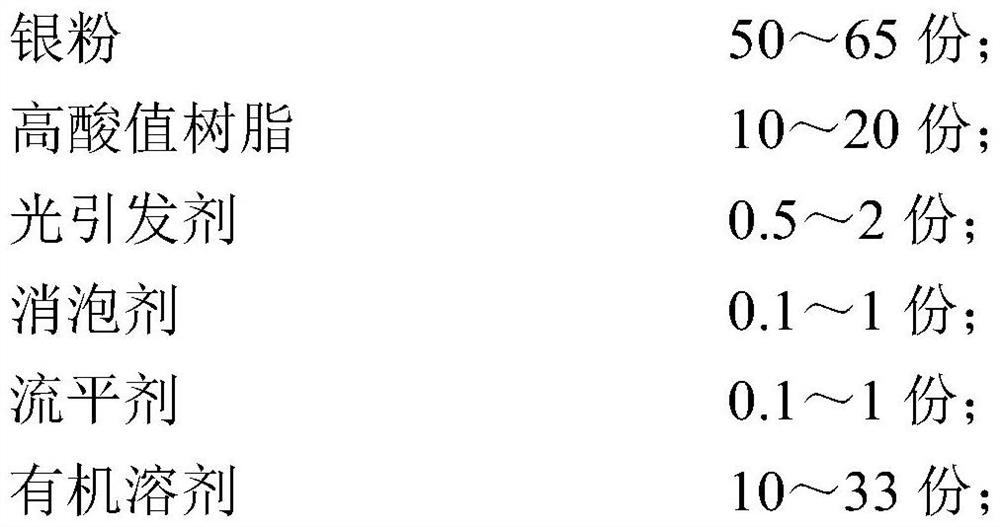
The invention discloses conductive ink with a circuit etching performance, as well as a preparation method and application thereof. The conductive ink comprises the following components in percent bymass: 50 to 65 parts of silver powder, 10 to 20 parts of high acid value resin, 0.5 to 2 parts of a photoinitiator, 0.1 to 1 part of a defoamer, 0.1 to 1 part of a flatting agent, and 10 to 33 parts of an organic solvent. The conductive ink can be applied to a printed circuit board: all the components are uniformly mixed through ultrasound, so that the conductive ink is obtained; then the conductive ink is applied onto a substrate and dried; a photomask is used for covering to perform photocuring; finally the photomask is removed, and developing and drying are performed, so that a conducting circuit is obtained. The conductive ink is simple in technology, equipment and material costs are reduced, energy can be saved, chemical liquid waste is not produced and no environmental pollution is caused, so that market requirements are greatly met.

Description

technical field [0001] The invention belongs to the field of conductive ink material preparation, and in particular relates to a conductive ink with circuit etching performance and a preparation method and application thereof. Background technique [0002] Conductive ink is a conductive composite material formed by dispersing metal conductive particles (silver, copper, carbon, usually silver) in a binder. After printing on the substrate, it acts as a wire, antenna and resistor. Conductive ink is the most basic and critical raw material for the production of organic printed circuit boards (thin films). One of the key raw materials for the success of organic printed electronic products. [0003] In recent years, the information, communication and consumer electronics industries have developed rapidly. In the information, communication and consumer electronics industries, printed circuit boards are an indispensable and important component. The traditional process of manufact...

Claims


Application Information

Patent Timeline
Patent Type & Authority Patents(China)
IPC IPC(8): C09D11/52C09D11/101G03F7/027H05K3/06
CPCC09D11/101C09D11/52G03F7/027H05K3/06H05K2203/052
Inventor 吕满庚陈国康吴昆
Owner NANXIONG MATERIAL PRODION BASE OF CHINESE ACADEMY OF SCI GUANGZHOU CHEM
Learn More