Processing method and electronic device

A technology of electronic equipment and processing method, which is applied in the directions of digital output to display equipment, acquisition/organization of fingerprints/palmprints, printing image collection, etc., which can solve the problem of occupying the structural space of electronic equipment and the slim form of electronic equipment that cannot meet the pursuit of users , Reduce user experience and other issues, achieve the effect of improving user experience, saving structural space, and convenient and quick operation

Pending Publication Date: 2018-02-23
LENOVO (BEIJING) LTD
View PDF7 Cites 26 Cited by
  • Summary
  • Abstract
  • Description
  • Claims
  • Application Information

AI Technical Summary

Problems solved by technology

[0004] However, in the prior art, when the electronic device is provided with the fingerprint recognition module, it is usually separately arranged on a part other than the display screen, that is, it is separated from the display screen and becomes two independent parts. Occupying the structural space of electronic equipment makes the electronic equipment unable to meet the slim form pursued by users and reduces the user experience

Method used


Image

  • Processing method and electronic device
  • Processing method and electronic device
  • Processing method and electronic device

Examples


Embodiment 1

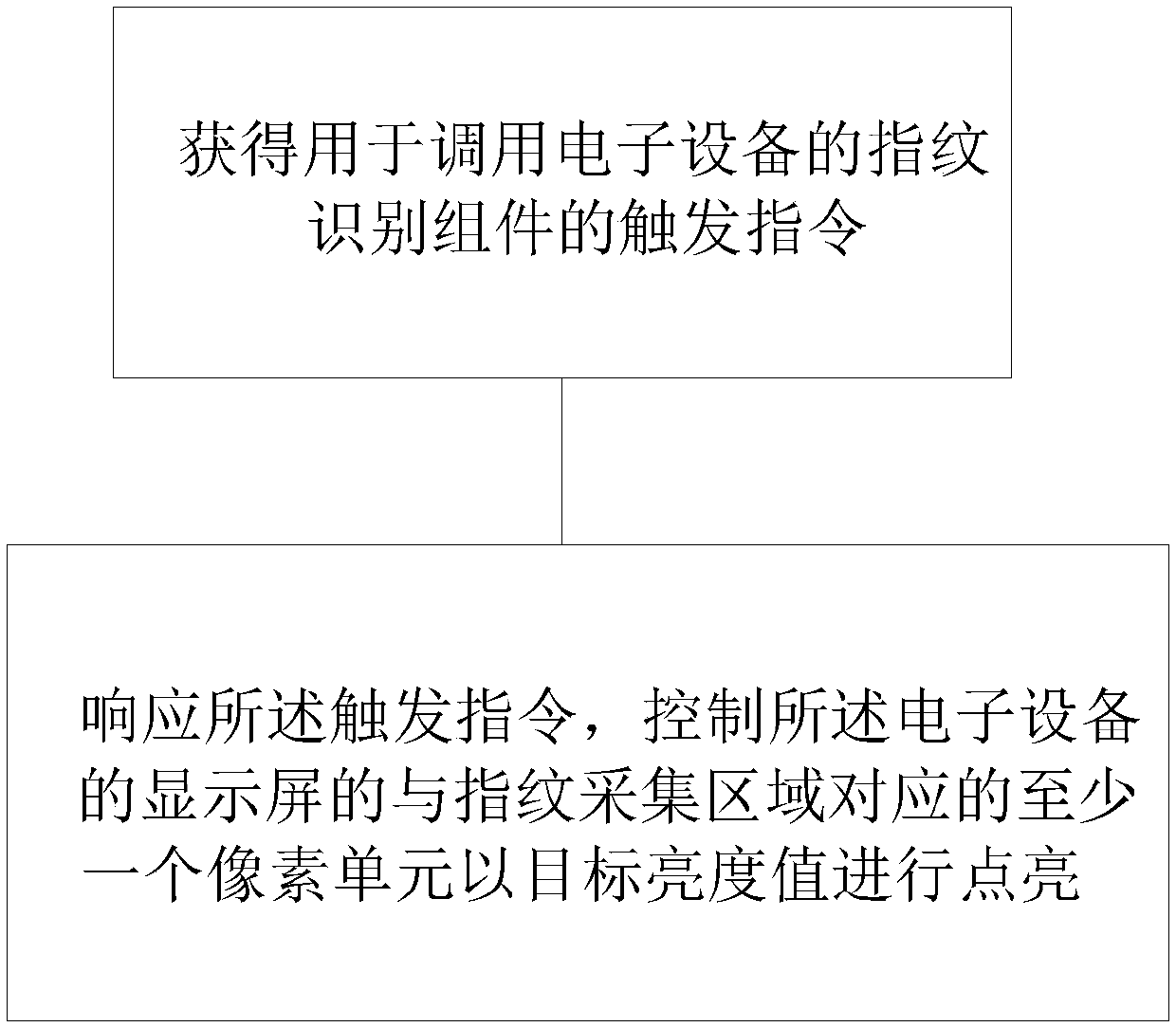
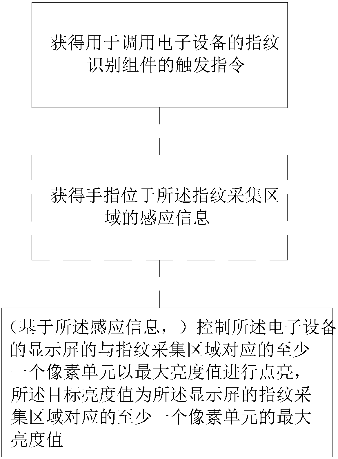
[0080] Embodiment one, such as figure 2 Shown:

[0081] Controlling at least one pixel unit corresponding to the fingerprint collection area of ​​the display screen of the electronic device to light up with a maximum brightness value, and the target brightness value is the maximum brightness value of at least one pixel unit corresponding to the fingerprint collection area of ​​the display screen; that is, as long as After the system obtains the trigger command, it controls at least one pixel unit of the display screen corresponding to the fingerprint collection area to light up with the maximum brightness value (the default display screen has not been lit beforehand), so that the current brightness value of the pixel unit is the maximum value , while the pixel units in the rest of the display are lit with the original lighting current. If the display screen has been lit in advance, adjust the current brightness value of at least one pixel unit corresponding to the fingerprin...

Embodiment 2

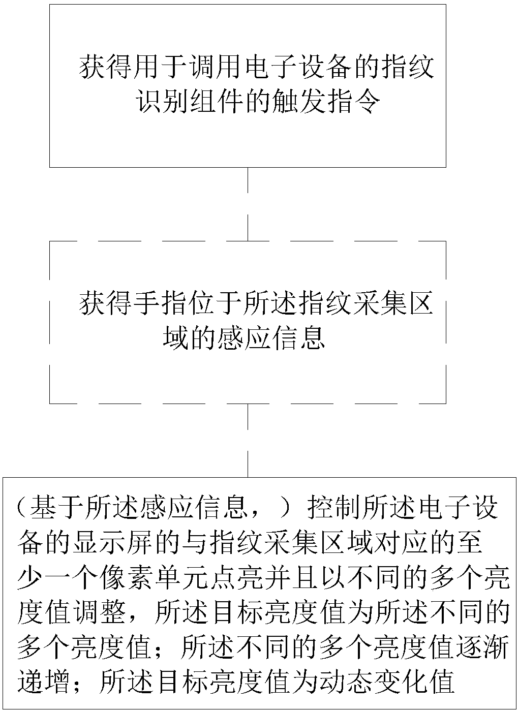
[0085] Embodiment two, such as image 3 Shown:

[0086] Controlling at least one pixel unit corresponding to the fingerprint collection area of ​​the display screen of the electronic device to light up and adjust with multiple different brightness values, the target brightness value is multiple different brightness values; the multiple different brightness values ​​gradually increase; the target The brightness value is a dynamically changing value. This embodiment refers to that after the system acquires the trigger instruction, it first lights up at least one pixel unit of the display screen corresponding to the fingerprint collection area with a minimum brightness value or a preset initial brightness value, and lasts for a period of time, that is, , the pixel unit is displayed at this brightness value for a period of time, for example, for 2s or 3s, etc., and then re-lights the above pixel unit with a slightly higher than the minimum brightness value or the initial brightne...

Embodiment 3

[0091] Embodiment three, such as Figure 4 Shown:

[0092] Obtain the sensing information that the finger is located in the fingerprint collection area, that is, the user needs to place the finger on the part of the display screen corresponding to the fingerprint collection area, and the trigger command can be generated by the user clicking the part of the display screen corresponding to the fingerprint collection area. After lighting up the display screen in other ways, place your finger on the part of the display screen corresponding to the fingerprint collection area;

[0093] Based on the sensing information, controlling at least one pixel unit of the display screen of the electronic device corresponding to the fingerprint collection area to light up with a first brightness value;

[0094]Obtain the collection result of the identification module, that is, the fingerprint image formed after the identification module collects the fingerprint;

[0095] Based on the collecti...


PUM


Abstract

An embodiment of the invention discloses a processing method and an electronic device. The method includes the steps: acquiring a triggering instruction of a fingerprint identification component for calling the electronic device; responding the triggering instruction, and controlling at least one pixel unit of a display screen of the electronic device corresponding to a fingerprint acquisition area to be illumined by the aid of a target luminance value; taking at least one illumined pixel unit of the display screen positioned in the fingerprint acquisition area as a light source of the fingerprint identification module, and enabling a finger needle to generate reflection light for at least one illumined pixel unit when a finger is positioned in the fingerprint acquisition area. An identification module of the fingerprint identification component is positioned below a display screen, corresponds to the fingerprint acquisition area and used for receiving the reflection light to acquire afingerprint. According to the processing method, part of or all display area of the display screen can be automatically adjusted according to instructions of a user and serves as the fingerprint acquisition area capable of acquiring fingerprints, and a fingerprint acquisition area additionally arranged outside the display screen of the electronic device is omitted.

Description

technical field [0001] The invention relates to the field of intelligent equipment control, in particular to a processing method and electronic equipment applying the processing method. Background technique [0002] Fingerprint, because of its lifelong invariance, uniqueness and convenience, has almost become synonymous with biometric identification. Fingerprints are the uneven lines on the skin at the end of a person's fingers. The lines are arranged regularly to form different grain types. The starting point, ending point, joint point and bifurcation point of the ridge line are called the detail feature points of the fingerprint. [0003] Fingerprint identification usually adopts optical fingerprint identification method. The principle is: set a light source under the display screen, so that the light source emits light to the outside of the display screen. Through the pixel layer of the display screen, it reaches the optical fingerprint sensor, so that the system can i...

Claims


Application Information

Patent Timeline
Patent Type & Authority Applications(China)
IPC IPC(8): G06F3/14G06K9/00G06V10/141
CPCG06F3/14G06V40/13G09G2360/144G09G2320/0686G09G2354/00G09G3/32G06V40/1312G06V10/141G09G5/10G09G2320/0626G06V40/1318
Inventor 卢正鎏钱明贵
Owner LENOVO (BEIJING) LTD
Why Eureka
Try Eureka