Substrate, preparation method thereof, display panel and display device

A substrate and display area technology, which is applied in semiconductor/solid-state device manufacturing, electrical components, electric solid-state devices, etc., can solve the problem of uneven unevenness of the flat layer

Active Publication Date: 2018-02-23
BOE TECH GRP CO LTD +1
View PDF5 Cites 7 Cited by
  • Summary
  • Abstract
  • Description
  • Claims
  • Application Information

AI Technical Summary

Problems solved by technology

[0005] Embodiments of the present invention provide a substrate and its preparation method, a display panel, and

Method used


Image

  • Substrate, preparation method thereof, display panel and display device
  • Substrate, preparation method thereof, display panel and display device
  • Substrate, preparation method thereof, display panel and display device

Examples


Embodiment Construction

[0032] The following will clearly and completely describe the technical solutions in the embodiments of the present invention with reference to the accompanying drawings in the embodiments of the present invention. Obviously, the described embodiments are only some, not all, embodiments of the present invention. Based on the embodiments of the present invention, all other embodiments obtained by persons of ordinary skill in the art without making creative efforts belong to the protection scope of the present invention.

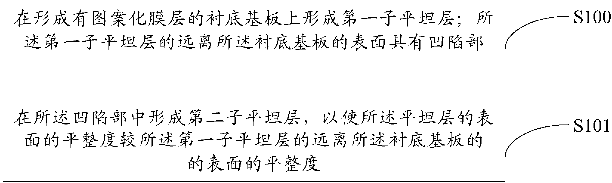
[0033] An embodiment of the present invention provides a method for preparing a substrate, including: forming a flat layer; wherein, forming a flat layer includes: such as figure 2 as shown,

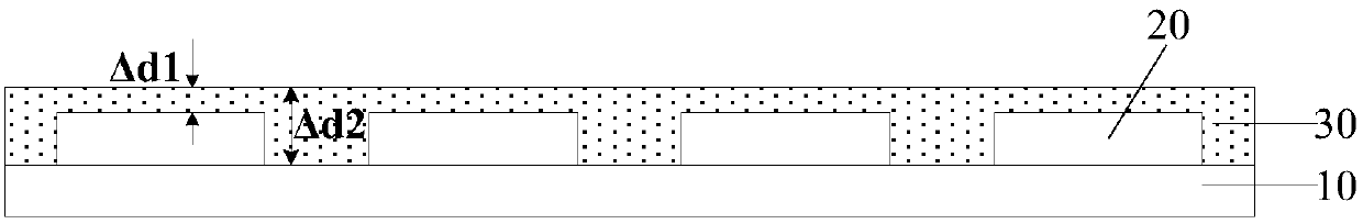
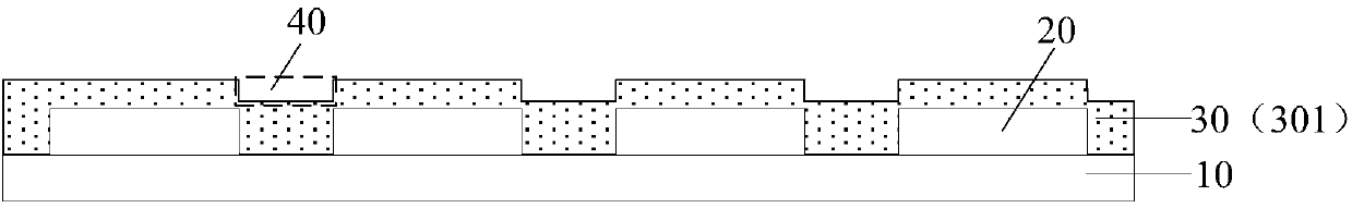
[0034] S100, as shown in FIG. 1(b), form a first sub-planar layer 301 on the base substrate 10 on which the patterned film layer 20 is formed; the surface of the first sub-planar layer 301 away from the base substrate 10 has a concave portion 40.

[0035] Wherein, the...


PUM


Abstract

The embodiment of the invention provides a substrate, a preparation method thereof, a display panel and a display device, relates to the technical field of display, and is used for solving the problemthat a flat layer is rugged in the manufacturing process. The preparation method comprises the following steps: forming the flat layer, wherein the step of forming the flat layer comprises forming afirst sublayer on a substrate on which a patterned film is formed, wherein the surface, away from the substrate, of the first sublayer is provided with a concave part; and forming a second sublayer inthe concave part so that the flatness of the surface of the flat layer is higher than that of the surface, away from the substrate, of the first sublayer. The preparation method is used for forming the flat layer.

Description

technical field [0001] The invention relates to the field of display technology, in particular to a substrate and a preparation method thereof, a display panel, and a display device. Background technique [0002] At present, with the rapid development of science and technology, various display devices are gradually developed, for example, liquid crystal display (Liquid Crystal Display, LCD for short), organic light-emitting diode display (Organic Light-Emitting Diode Display, OLED for short) . [0003] Whether it is an LCD display device or an OLED display device, a flat layer is often formed during the manufacturing process. If the flatness of the flat layer is not enough, unevenness is likely to appear in the pixel, which will seriously affect the performance of the display device. [0004] Taking OLED display devices as an example, the film-forming methods of organic electroluminescent devices mainly include solution process, and the film-forming methods of solution proc...

Claims


Application Information

Patent Timeline
IPC IPC(8): H01L27/32H01L21/77
CPCH10K59/122H10K59/1201H01L27/1248H10K59/124H01L27/1262
Inventor 贾文斌王辉锋廖金龙朱飞飞万想
Owner BOE TECH GRP CO LTD
Why Eureka
Try Eureka