
Chip trimming circuit and chip trimming method

A technology for trimming and adjusting circuits and chips, which is applied in the direction of logic circuits, logic circuit interface devices, logic circuit connection/interface layout, etc., and can solve problems such as poor trimming results, unblown fuses, and wrong fuse trimming, etc., to achieve Reliable trimming and improved accuracy

Active Publication Date: 2018-02-27
저장진셍일렉트로닉스테크놀러지컴퍼니리미티드
View PDF4 Cites 5 Cited by
  • Summary
  • Abstract
  • Description
  • Claims
  • Application Information

AI Technical Summary

Problems solved by technology

Since the fuse blowing process has requirements for the voltage, current and duration applied to the fuse, if the voltage, current and duration of the fuse are not well controlled, there will be a normal distribution of the impedance after the fuse is blown , therefore, the traditional fuse trimming has a certain probability of trimming errors
In addition, if the current or voltage selection of the blown fuse in the design is unreasonable, it will also lead to the situation that the fuse is not blown. If the fuse is not blown, the purpose of accurate trimming cannot be achieved, and the trimming result will even be worse.
Therefore, the traditional fuse trimming method is not ideal for trimming the test parameters of the chip, so it cannot improve the accuracy of the test parameters and the yield of the chip.

Method used


Image

  • Chip trimming circuit and chip trimming method
  • Chip trimming circuit and chip trimming method
  • Chip trimming circuit and chip trimming method

Examples


Embodiment Construction

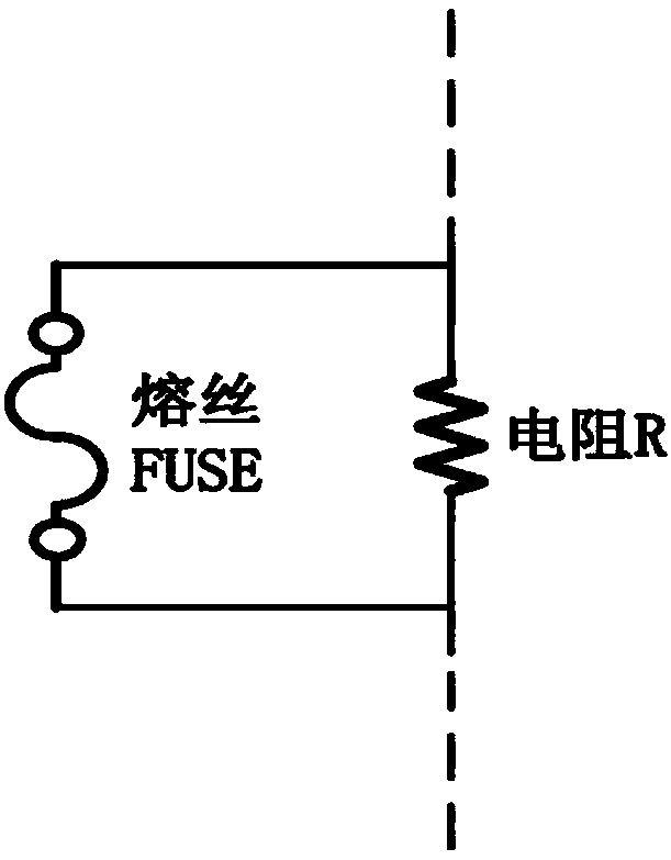
[0034] In order to make the purpose, technical solutions and advantages of the application clearer, the application will be further described in detail below in conjunction with the accompanying drawings. Obviously, the described embodiments are only some of the embodiments of the application, not all of them. . Based on the embodiments in this application, all other embodiments obtained by persons of ordinary skill in the art without making creative efforts belong to the scope of protection of this application.

[0035] In this application, there is no limitation on how to obtain the test parameters of the chip. For example, the test parameters may be obtained by testing the key parameters of the chip, or may be obtained by testing all the parameters of the chip.

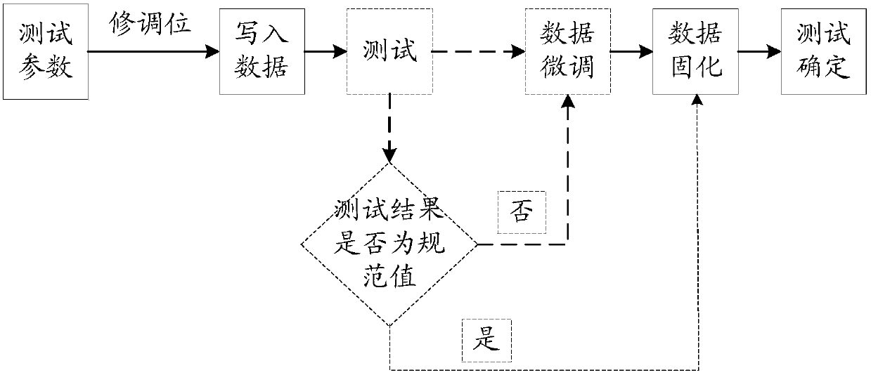
[0036] The chip trimming circuit provided by this application can be applied to image 3 In the test scenario shown, such as image 3 As shown, after obtaining the test parameters, by looking up the corresponding...


PUM


Abstract

The invention discloses a chip trimming circuit and a chip trimming method for solving the problem of relatively low precision of test parameters of chips due to unreliable trimming of the chips in the prior art. The chip trimming circuit comprises a trimming control module, a curing circuit module and an output circuit module, the curing circuit module comprises a first curing sub-module, a second curing sub-module and a burning control sub-module for controlling to burn the first curing sub-module and the second curing sub-module, the trimming control module is used for outputting a trimmingposition determined according to the test parameters of a chip to the curing circuit module, the curing circuit module is used for controlling the burning control sub-module to burn the first curingsub-module or the second curing sub-module according to the trimming position and converting the trimming position into a resistance change corresponding to the burnt curing sub-module after the burning, and the output circuit module is used for outputting a logic level signal according to the resistance change.

Description

technical field [0001] The present application relates to the field of circuit control, in particular to a chip trimming circuit and trimming method. Background technique [0002] With the development of integrated circuit design and process technology, the requirements for circuit performance in the chip production process are getting higher and higher. Due to the process deviation of the chip in the production process, there is a deviation between the performance index of the chip parameter and the expected parameter performance index, which affects the accuracy of the chip parameter. Some chip parameters may exceed the range required by the product specification, thus affecting If the yield rate of the chip is serious, the chip cannot be mass-produced. In order to improve the accuracy of the chip parameters and the yield rate of the chip, the chip parameters are usually tested during the production process of the chip or after the chip production is completed, and then t...

Claims


Application Information

Patent Timeline
IPC IPC(8): H03K19/00H03K19/0175
CPCH03K19/0005H03K19/017509
Inventor 朱海刚李龙弟方伟
Owner 저장진셍일렉트로닉스테크놀러지컴퍼니리미티드
Learn More