Supercharge Your Innovation With Domain-Expert AI Agents!

High voltage diode employing aluminum copper alloy for electrode structure and bridging structure and preparation method of high voltage diode

A high-voltage diode and bridge structure technology, which is applied in the direction of circuits, electrical components, and electrical solid devices, can solve problems such as chip leakage and dead lights, and achieve the effect of solving the phenomenon of chip electrode electromigration

Active Publication Date: 2018-03-06
JIANGSU XGL OPTOELECTRONICS
View PDF4 Cites 3 Cited by
  • Summary
  • Abstract
  • Description
  • Claims
  • Application Information

AI Technical Summary

Problems solved by technology

[0004] In order to solve the electromigration problem existing in the electrodes of traditional high-voltage diodes, the present invention provides a high-voltage diode based on an aluminum-copper alloy as the electrode structure and bridge structure, which can solve the problems of chip leakage and dead lights in pure aluminum high-voltage diodes

Method used


Image

  • High voltage diode employing aluminum copper alloy for electrode structure and bridging structure and preparation method of high voltage diode
  • High voltage diode employing aluminum copper alloy for electrode structure and bridging structure and preparation method of high voltage diode

Examples


Embodiment 1

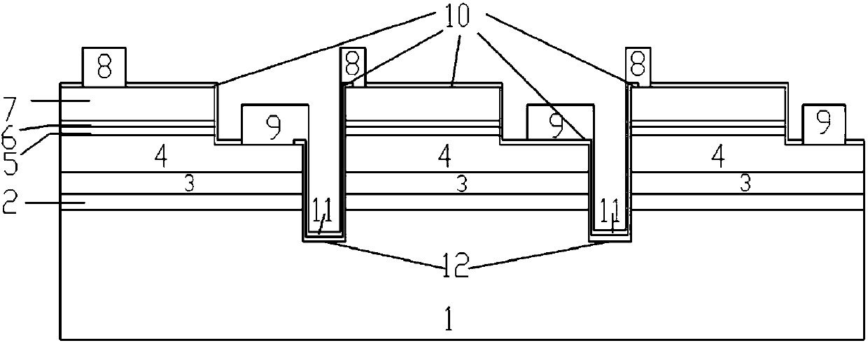
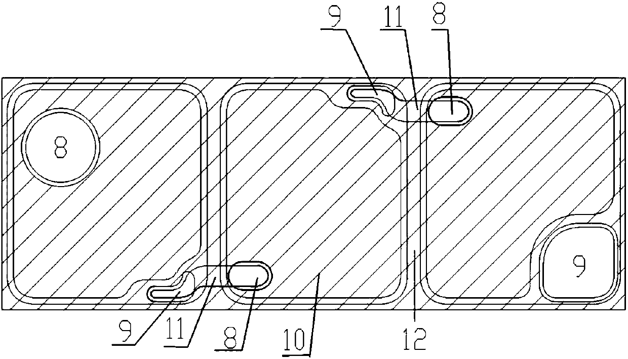
[0030] Example 1, when the bridge structure 11, the N electrode 9 and the P electrode 8 are all made of an aluminum-copper alloy with a copper content of 0.5%, within 96 hours of electrode aging, there is no precipitate at the electrode and the bridge structure, and the bridge The change values ​​of the forward voltage of structure 11, N electrode 9 and P electrode are all close to 0V, and no precipitate can be reflected. Electromigration did not occur in the electrode and bridge structure within 96 hours of the aging test.

Embodiment 2

[0031] Example 2, when the bridge structure 11, the N electrode 9 and the P electrode 8 are all made of an aluminum-copper alloy with a copper content of 2%, within 96 hours of electrode aging, there is no precipitate at the electrode and the bridge structure, and the bridge The change values ​​of the forward voltage of structure 11, N electrode 9 and P electrode are all close to 0V, and no precipitate can be reflected. Electromigration did not occur in the electrode and bridge structure within 96 hours of the aging test.

[0032] A manufacturing process based on an aluminum-copper alloy as an electrode structure and a bridging structure, comprising the following steps:

[0033] Step 1: growing the buffer layer 2, U-GaN layer 3, N-GaN layer 4, multi-quantum hydrazine 5 and P-GaN layer 6 sequentially from bottom to top on the substrate 1 to form an LED epitaxial wafer;

[0034] Step 2: cleaning the LED epitaxial wafer, sputtering ITO on the surface of the P-GaN layer 6 to form ...


PUM


Abstract

The invention provides a high voltage diode employing aluminum copper alloy for an electrode structure and a bridging structure. The high voltage diode includes a substrate. A plurality of light emitting units are arranged on the substrate. Neighboring light emitting units are isolated by channels. Each light emitting unit includes a buffer layer, a U-GaN layer, an N-GaN layer, a multi-quantum well, a P-GaN layer and an ITO layer arranged successively from bottom up on the substrate. The upper surface of the N-GaN layer is exposed partially. The surface of each channel is provided with an insulation layer. The exposed support surface of the N-GaN layer of each light emitting unit is provided with an N electrode and an insulation layer. The upper surface of the ITO layer of each light emitting unit is provided with a P electrode and an insulation layer. In two neighboring light emitting units, a bridging structure is arranged on the upper surface of the insulation layer between a P electrode of one light emitting unit and the N electrode of the other light emitting unit. The high voltage diode can solve problems of chip electric leakage and LED damage of a pure aluminum electrode high voltage diode.

Description

technical field [0001] The invention relates to a high-voltage diode, in particular to a high-voltage diode based on an aluminum-copper alloy as an electrode structure and a bridge structure and a preparation method thereof. Background technique [0002] Now the high-voltage light-emitting diode (HV LED) is widely used in the market. This HV LED is composed of multiple light-emitting units isolated from each other until the groove of the growth substrate, and is connected to the N welding of two adjacent light-emitting units by a bridge structure. Between the P pad and the P pad, multiple light-emitting units are connected in series. Now the market mostly uses Cr / Al / Cr / Pt / Au structures as the electrode structure and bridge structure. The main reason why HV LEDs choose aluminum is because it has a low High resistivity, high specular reflectivity, and its cost is quite low. [0003] Traditional high-voltage diodes usually have a pure aluminum metal layer. However, the pure al...

Claims


Application Information

Patent Timeline
IPC IPC(8): H01L27/15H01L33/40H01L23/532H01L33/00H01L21/768
CPCH01L21/76838H01L23/53219H01L27/153H01L33/0075H01L33/40H01L2933/0016
Inventor 闫晓密黄慧诗华斌
Owner JIANGSU XGL OPTOELECTRONICS
Features
  • R&D
  • Intellectual Property
  • Life Sciences
  • Materials
  • Tech Scout
  • Unparalleled Data Quality
  • Higher Quality Content
  • 60% Fewer Hallucinations
Learn More