High-voltage diode with aluminum-copper alloy electrode structure and bridge structure and preparation method thereof
A high-voltage diode and bridge structure technology, which is applied in the direction of circuits, electrical components, and electrical solid devices, can solve problems such as chip leakage and dead lights, and achieve the effect of solving the phenomenon of chip electrode electromigration
- Summary
- Abstract
- Description
- Claims
- Application Information
AI Technical Summary
Problems solved by technology
Method used
Image
Examples
Embodiment 1
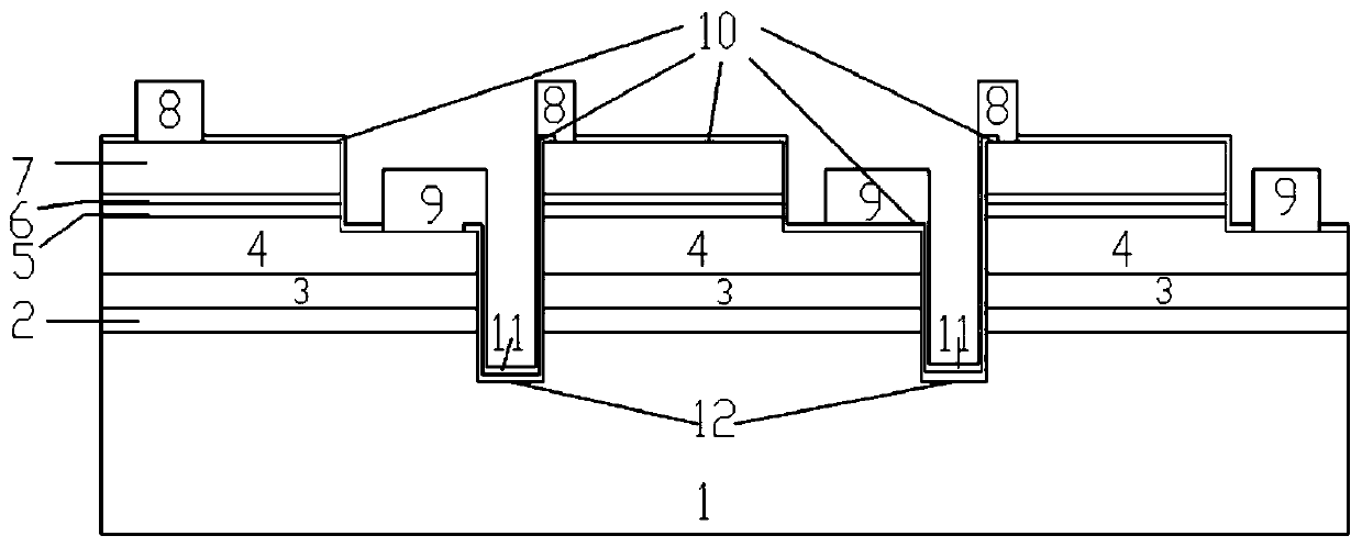
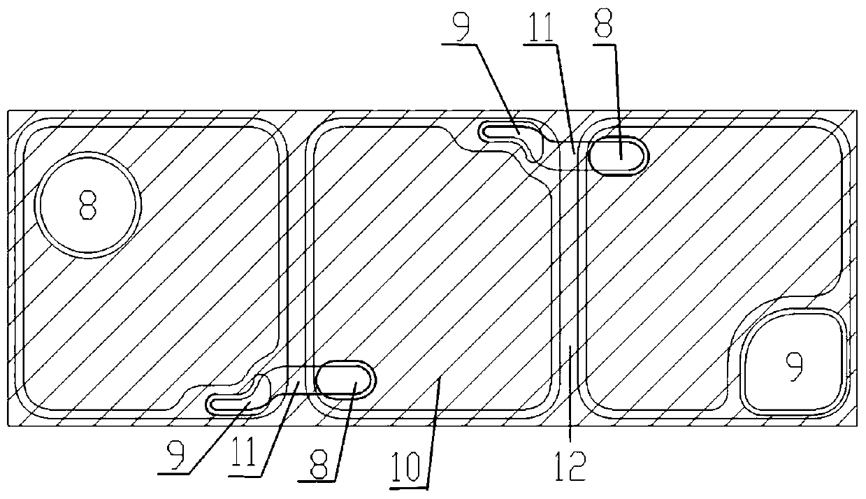
[0030] Example 1, when the bridge structure 11, the N electrode 9 and the P electrode 8 are all made of an aluminum-copper alloy with a copper content of 0.5%, within 96 hours of electrode aging, there is no precipitate at the electrode and the bridge structure, and the bridge The change values of the forward voltage of structure 11, N electrode 9 and P electrode are all close to 0V, and no precipitate can be reflected. Electromigration did not occur in the electrode and bridge structure within 96 hours of the aging test.
Embodiment 2
[0031] Example 2, when the bridge structure 11, the N electrode 9 and the P electrode 8 are all made of an aluminum-copper alloy with a copper content of 2%, within 96 hours of electrode aging, there is no precipitate at the electrode and the bridge structure, and the bridge The change values of the forward voltage of structure 11, N electrode 9 and P electrode are all close to 0V, and no precipitate can be reflected. Electromigration did not occur in the electrode and bridge structure within 96 hours of the aging test.
[0032] A manufacturing process based on an aluminum-copper alloy as an electrode structure and a bridging structure, comprising the following steps:
[0033] Step 1: growing the buffer layer 2, U-GaN layer 3, N-GaN layer 4, multi-quantum hydrazine 5 and P-GaN layer 6 sequentially from bottom to top on the substrate 1 to form an LED epitaxial wafer;
[0034] Step 2: cleaning the LED epitaxial wafer, sputtering ITO on the surface of the P-GaN layer 6 to form ...
PUM
 Abstract
Description
Claims
Application Information
 - R&D
- Intellectual Property
- Life Sciences
- Materials
- Tech Scout
- Unparalleled Data Quality
- Higher Quality Content
- 60% Fewer Hallucinations
Browse by: Latest US Patents, China's latest patents, Technical Efficacy Thesaurus, Application Domain, Technology Topic, Popular Technical Reports.
© 2025 PatSnap. All rights reserved.Legal|Privacy policy|Modern Slavery Act Transparency Statement|Sitemap|About US| Contact US: help@patsnap.com


