Microstrip transmission device and preparation method

A technology of microstrip transmission and microstrip transmission line, which is applied in the direction of waveguide devices, electrical components, waveguides, etc., can solve the application limitations of high-frequency signal shielding transmission, cannot achieve miniaturization production requirements, and cannot achieve isolation well Transmission and other issues, to achieve the effect of controllable hole wall roughness, high-performance transmission satisfaction, and low cost

Pending Publication Date: 2020-04-17
成都迈科科技有限公司
View PDF0 Cites 2 Cited by
  • Summary
  • Abstract
  • Description
  • Claims
  • Application Information

AI Technical Summary

Problems solved by technology

If the through-silicon via technology TSV is used to make signal shielding vias, since silicon is a semiconductor material with low resistivity, electrons around TSV can move freely under the action of an electromagnetic field, which will affect adjacent signals and cannot achieve good isolation. Transmission, affecting chip performance
If the ceramic through-hole technology TCV is used, the ceramic is mainly drilled with a laser. The minimum hole diameter is 150 μm and the pitch is 250 μm. Therefore, the minimum center-to-center spacing of the holes is 400 μm. It is difficult to produce high-density through holes and cannot achieve good isolation transmission. , the roughness of the side wall of the hole is also difficult to meet the requirements, and the strength of ceramic laser drilling will be greatly reduced, and the production requirements of miniaturization cannot be achieved, so its application in high-frequency signal shielding transmission has great limitations

Method used


Image

  • Microstrip transmission device and preparation method
  • Microstrip transmission device and preparation method
  • Microstrip transmission device and preparation method

Examples


Embodiment Construction

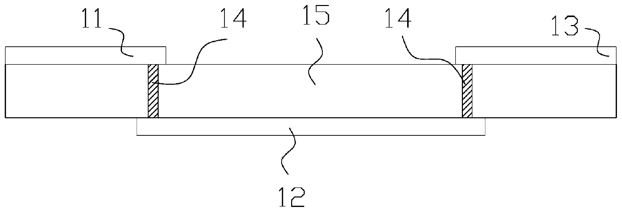
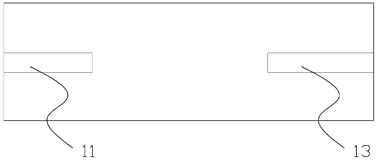
[0034] figure 1 It is a structural schematic diagram of the prior art, which has no isolation holes. figure 2 show figure 1 A schematic view of the state of looking up in the prior art shown. figure 1 Among them, 11 is section A of the microstrip transmission line, 12 is section B of the microstrip transmission line, 13 is section C of the microstrip transmission line, 14 is a metallized via hole, and 15 is a substrate.

[0035] image 3 It is a structural schematic diagram of the present invention, Figure 4 For looking up state. 41 is section A of the microstrip transmission line, 42 is section B of the microstrip transmission line, 43 is section C of the microstrip transmission line, 44 is a metallized via hole, 45 is a glass substrate, and 46 is a shielding hole. Figure 4 It shows the looking up state, and the shielding holes are arranged on both sides of the microstrip transmission line. Since the shielding hole is a metallized through hole, see the top view Fig...


PUM

PropertyMeasurementUnit
diameteraaaaaaaaaa

Abstract

The invention discloses a microstrip transmission device and a preparation method, which relate to an electronic device, and particularly design a microstrip transmission line. The microstrip transmission device comprises a substrate and a microstrip line arranged on the surface of the substrate, and is characterized in that the substrate is a glass substrate, a column of metallized through holespenetrating through the substrate is formed in each of two sides of the microstrip transmission line along the trend of the microstrip transmission line, and the metallized through holes are used as shielding holes. The high-frequency signal shielding hole is made of photolithographic glass, and compared with a TSV technology, an insulating layer does not need to be made, and the electromigrationphenomenon is avoided.

Description

technical field [0001] The present invention relates to electronic devices, in particular to microstrip transmission lines. Background technique [0002] With the development of IC chips in the direction of nanometers, people have higher and higher requirements for small size, light weight and high reliability of chips. The wire bonding technology used in traditional 2D packaging requires long-distance interconnection, the delay of the circuit is relatively large and the circuit is prone to failure, and the overall quality and volume of the circuit system are also relatively large. The development trend of miniaturization and high integration of electronic products requires corresponding nano-packaging technology, and through-hole interconnection technology is undoubtedly a cost-effective and high-reliability interconnection packaging technology. [0003] Now commonly used high-frequency signal shielding holes mostly use silicon or ceramics as substrates. If the through-si...

Claims


Application Information

Patent Timeline
Patent Type & Authority Applications(China)
IPC IPC(8): H01P3/08H01P11/00H01L23/66
CPCH01L23/66H01L2223/6627H01P3/081H01P11/003
Inventor 奉建华王文君林彬穆俊宏
Owner 成都迈科科技有限公司
Why Eureka
Try Eureka