Display substrate and preparation method therefor and display panel

A display substrate and substrate substrate technology, applied in the direction of electrical components, electrical solid devices, circuits, etc., can solve problems such as poor working stability, easy drift of thin-film transistor threshold voltage, thin-film transistor threshold voltage shift, etc., to ensure work The effect of stability

Pending Publication Date: 2018-03-06
BOE TECH GRP CO LTD
View PDF10 Cites 16 Cited by
  • Summary
  • Abstract
  • Description
  • Claims
  • Application Information

AI Technical Summary

Problems solved by technology

However, due to the reflective effect of the metal film, when part of the light generated by the light-emitting element hits the surface of the metal film (the side surface facing away from the substrate), this part of the light will be reflected on the surface of the metal film and direc

Method used


Image

  • Display substrate and preparation method therefor and display panel
  • Display substrate and preparation method therefor and display panel
  • Display substrate and preparation method therefor and display panel

Examples


Embodiment Construction

[0044] In order for those skilled in the art to better understand the technical solution of the present invention, the display substrate provided by the present invention, its manufacturing method, and the display panel are described in detail below with reference to the accompanying drawings.

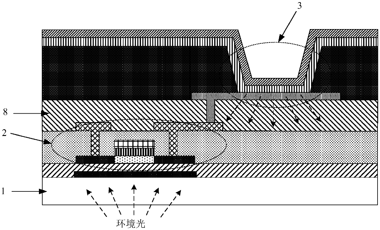
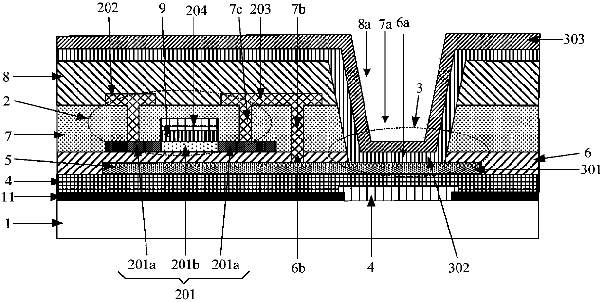
[0045] figure 2 A schematic cross-sectional view of a display substrate provided in Embodiment 1 of the present invention, as shown in figure 2 As shown, the display substrate includes: a base substrate 1, on which a thin film transistor 2 and a light emitting device are formed, and the thin film transistor 2 includes: a gate 204, an active layer 201, a source 202 and a drain 203, with An interlayer insulating layer 7 (Inner Layer Dielectric, ILD for short) is formed between the source layer 201, the source electrode 202, and the drain electrode 203, and the interlayer insulating layer 7 is provided with a first via hole 7a and a second via hole 7b to emit light. The device is locat...


PUM


Abstract

The invention discloses a display substrate and a preparation method therefor and a display panel. The display substrate comprises a substrate, wherein a thin film transistor and a light emitting device are formed on the substrate; the thin film transistor comprises an active layer, a source and a drain; an interlayer insulating layer is formed between the active layer and the source and between the active layer and the drain; a first via hole and a second via hole are formed in the interlayer insulating layer; the light emitting device is positioned in the first via hole; and the drain is connected with the positive electrode of the light emitting device through the second via hole. Compared with the prior art, by virtue of the technical scheme disclosed in the invention, a light emittingelement can be arranged in the first via hole in the interlayer insulating layer by changing the relative position between the thin film transistor and the light emitting element, so that the light emitting element and the thin film transistor can be positioned on the same height position of the substrate basically, thereby avoiding irradiation of the light from the light emitting element on theactive layer in the thin film transistor, and further ensuring working stability of the thin film transistor.

Description

technical field [0001] The invention relates to the field of display technology, in particular to a display substrate, a preparation method thereof, and a display panel. Background technique [0002] figure 1 It is a schematic cross-sectional view of a display substrate involved in the prior art, such as figure 1 As shown, the display substrate includes: a thin film transistor 2 and a light emitting element 3, wherein a passivation layer 8 is formed on the side of the thin film transistor 2 facing away from the base substrate 1, and the light emitting element 2 is located on the side of the passivation layer 8 facing away from the base substrate 1, the anode of the light emitting element 3 is connected to the drain of the thin film transistor 2 through the via hole on the passivation layer 8. [0003] In practical applications, it is found that since the light emitting element 3 is located on the side of the thin film transistor 2 facing away from the base substrate 1, th...

Claims


Application Information

Patent Timeline
IPC IPC(8): H01L27/32
CPCH10K59/123H10K59/12
Inventor 王国英宋振
Owner BOE TECH GRP CO LTD
Why Eureka
Try Eureka