

Semiconductor device and manufacturing method therefor and electronic apparatus
A manufacturing method and semiconductor technology, applied in semiconductor/solid-state device manufacturing, semiconductor devices, electric solid-state devices, etc., can solve problems affecting the mismatch performance of SRAM devices, achieve simple structure, improve mismatch performance, and eliminate aluminum diffusion Effect
- Summary
- Abstract
- Description
- Claims
- Application Information
AI Technical Summary
Problems solved by technology
Method used
Image

Examples
Embodiment 1
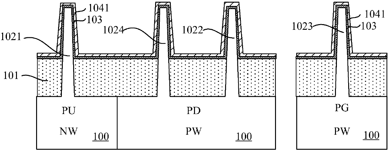
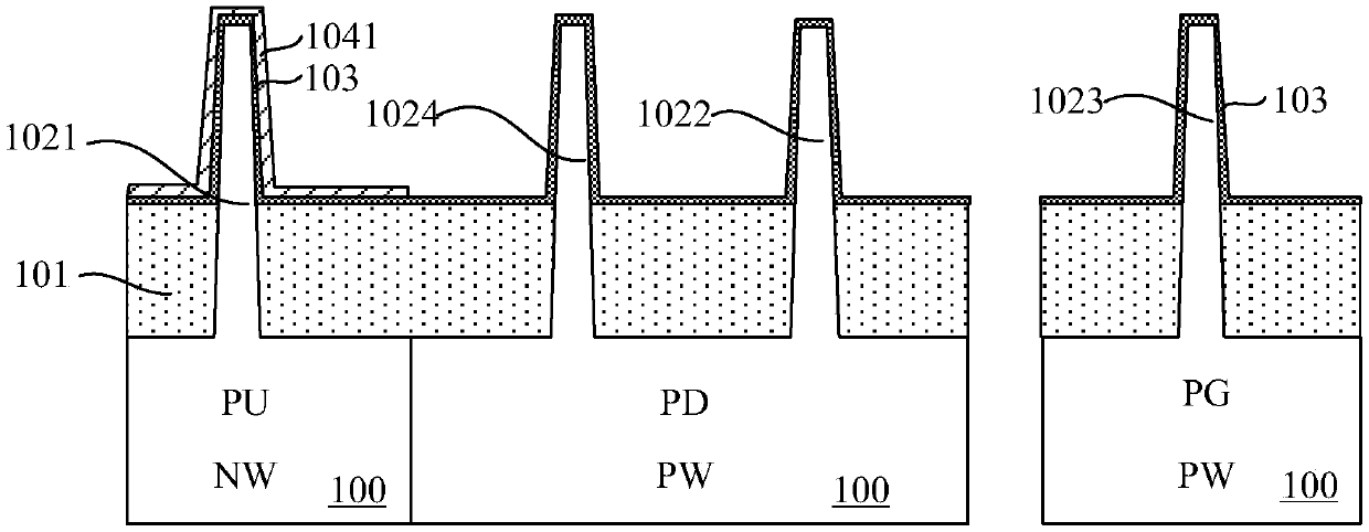
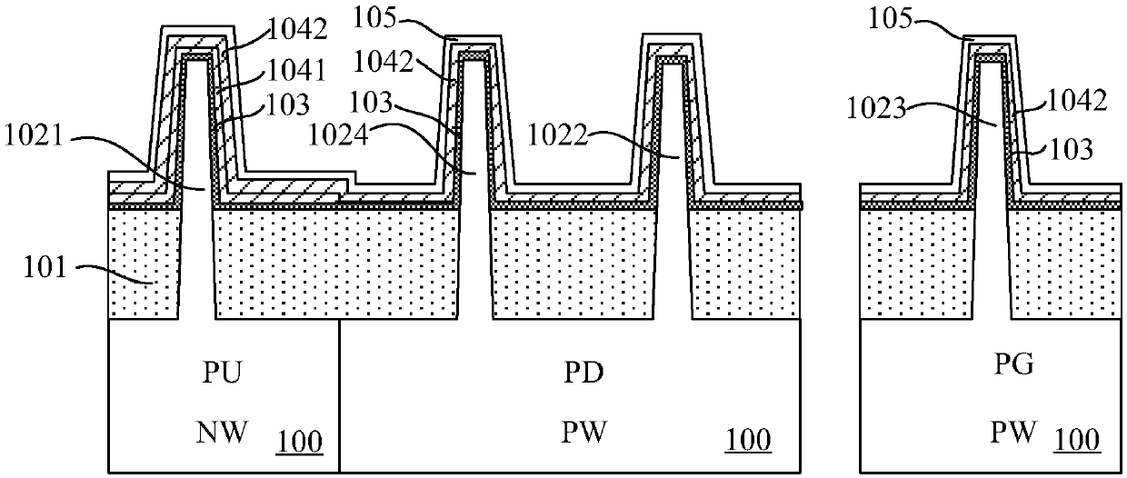
[0066] Below, refer to Figure 1A-Figure 1H The manufacturing method of the semiconductor device of the present invention is described in detail, wherein, Figure 1A-Figure 1H A cross-sectional view showing a structure formed in relevant steps of a method for manufacturing a semiconductor device in an embodiment of the present invention; figure 2 It shows a top view of a structure obtained by a method of manufacturing a semiconductor device in an embodiment of the present invention, and along figure 2 The structure obtained by the mid-section line and the Figure 1H Corresponds to the structure in .
[0067] Specifically, first, as Figure 1A As shown, a semiconductor substrate 100 is provided, and the semiconductor substrate 100 includes a pull-up transistor region, a pull-down transistor region, and a transfer gate transistor region, and the pull-up transistor region, the pull-down transistor region, and the pass-gate transistor region on the semiconductor substrate A fi...
Embodiment 2
[0145] The present invention also provides a semiconductor device formed by using the method in the first implementation, and the semiconductor device may be an SRAM device.
[0146] Below, refer to as Figure 1H and figure 2 The semiconductor device of the present invention will be described in detail.
[0147] First, the semiconductor device of the present invention includes: a semiconductor substrate 100, the semiconductor substrate 100 includes a pull-up transistor region, a pull-down transistor region and a transfer gate transistor region, the pull-up transistor region, A first fin structure 1021 , a second fin structure 1022 and a third fin structure 1023 are respectively formed in the pull-down transistor region and the transfer gate transistor region.
[0148] Wherein the semiconductor substrate 100 may include an active region for forming various constituent elements of the SRAM, for example, a PMOS device is formed in the pull-up transistor region, which acts as a...
Embodiment 3
[0185] The present invention also provides an electronic device, including the semiconductor device described in Embodiment 2, and the semiconductor device is prepared according to the method described in Embodiment 1.
[0186] The electronic device of this embodiment can be any electronic device such as a mobile phone, a tablet computer, a notebook computer, a netbook, a game console, a TV set, a VCD, a DVD, a navigator, a digital photo frame, a camera, a video camera, a recording pen, MP3, MP4, PSP, etc. Product or equipment, but also any intermediate product including electrical circuits. The electronic device of the embodiment of the present invention has better performance due to the use of the above circuit.
[0187] in, Figure 4 An example of a mobile phone handset is shown. The mobile phone handset 400 is provided with a display portion 402 included in a housing 401, operation buttons 403, an external connection port 404, a speaker 405, a microphone 406, and the lik...
PUM
| Property | Measurement | Unit |
|---|---|---|
| Thickness | aaaaa | aaaaa |
| Thickness | aaaaa | aaaaa |
| Thickness | aaaaa | aaaaa |
Abstract
Description
Claims
Application Information