A semiconductor device and its manufacturing method and electronic device

A manufacturing method and semiconductor technology, applied in semiconductor/solid-state device manufacturing, semiconductor devices, electric solid-state devices, etc., can solve problems such as poor device mismatch performance and large work function fluctuations

Active Publication Date: 2021-02-02
SEMICON MFG INT (SHANGHAI) CORP +1
View PDF5 Cites 0 Cited by
  • Summary
  • Abstract
  • Description
  • Claims
  • Application Information

AI Technical Summary

Problems solved by technology

[0003] In FinFET devices, the work function layer is very important for the adjustment of the device. In the device manufacturing process, the post-metal gate process is usually used to form the work function layer. In order to meet the different requirements of PMOS devices and NMOS devices for the work function layer, it is often necessary Multiple photolithography processes are carried out in the preparation process of the electrode. For example, in the SRAM device preparation process, it is often necessary to prepare a PMOS device as a pull-up transistor (PU) and an NMOS device as a pull-down transistor (PD). Different, after forming the P-type work function layer of the PMOS device, it is usually necessary to form a photoresist to cover the PMOS region through a photolithography process, to protect the P-type work function layer in the PMOS region, and then to etch the NMOS device region The inner P-type work function layer is removed, and then the photoresist is removed. During this process, residual impurities such as polymers will be generated, and these polymer impurities are easily left in the remaining P-type work function layer and diffusion barrier layer, etc. On the film layer, the fluctuation of the work function becomes larger, and the mismatch performance of the device becomes worse, especially for SRAM devices

Method used


Image

  • A semiconductor device and its manufacturing method and electronic device
  • A semiconductor device and its manufacturing method and electronic device
  • A semiconductor device and its manufacturing method and electronic device

Examples


Embodiment 1

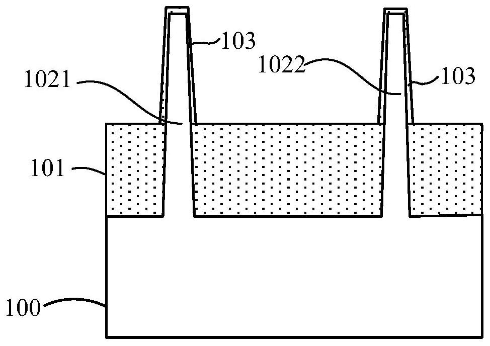
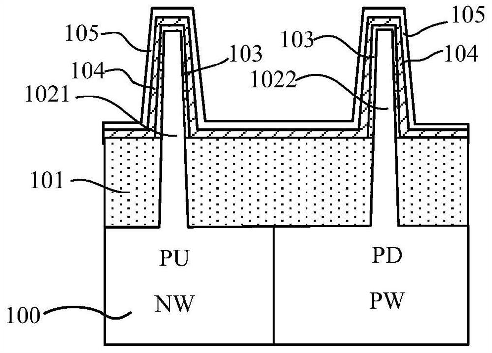
[0067] Below, refer to Figure 1A-Figure 1J The manufacturing method of the semiconductor device of the present invention is described in detail, wherein, Figure 1A-Figure 1J A cross-sectional view showing a structure formed in relevant steps of a method for manufacturing a semiconductor device in an embodiment of the present invention; figure 2 A top view of a structure obtained by a method for manufacturing a semiconductor device in an embodiment of the present invention is shown.

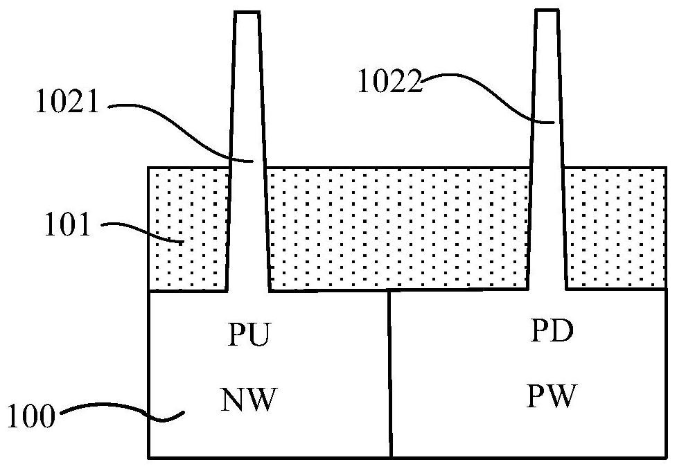
[0068] Specifically, first, as Figure 1A As shown, a semiconductor substrate 100 is provided, the semiconductor substrate 100 includes a PMOS region and an NMOS region, and a first fin structure 1021 is respectively formed in the PMOS region and the NMOS region on the semiconductor substrate 100 and the second fin structure 1022 .

[0069] In this example, the method of the present invention is described in detail by taking the manufacture of SRAM devices as an example, wherein, the PMOS regi...

Embodiment 2

[0136] The present invention also provides a semiconductor device formed by using the method in the first implementation, and the semiconductor device may be an SRAM device.

[0137] Below, refer to as Figure 1J and figure 2 The semiconductor device of the present invention will be described in detail.

[0138] First, the semiconductor device of the present invention includes: a semiconductor substrate 100, the semiconductor substrate 100 includes a PMOS region and an NMOS region, and first fins are respectively formed in the PMOS region and the NMOS region on the semiconductor substrate structure 1021 and a second fin structure 1022 .

[0139] When the semiconductor device is an SRAM device, the PMOS area refers to the pull-up transistor (PU) area of ​​the SRAM device, and the NMOS area refers to the down transistor (PD) area of ​​the SRAM device.

[0140] Further, various well regions are formed in the semiconductor substrate, for example, an N-type well region (NW) is ...

Embodiment 3

[0174] The present invention also provides an electronic device, including the semiconductor device described in Embodiment 2, and the semiconductor device is prepared according to the method described in Embodiment 1.

[0175] The electronic device of this embodiment can be any electronic device such as a mobile phone, a tablet computer, a notebook computer, a netbook, a game console, a TV set, a VCD, a DVD, a navigator, a digital photo frame, a camera, a video camera, a recording pen, MP3, MP4, PSP, etc. Product or equipment, but also any intermediate product including electrical circuits. The electronic device according to the embodiment of the present invention has better performance due to the use of the above-mentioned semiconductor device.

[0176] in, Figure 4 An example of a mobile phone handset is shown. The mobile phone handset 400 is provided with a display portion 402 included in a housing 401, operation buttons 403, an external connection port 404, a speaker 4...


PUM

PropertyMeasurementUnit
thicknessaaaaaaaaaa
thicknessaaaaaaaaaa
thicknessaaaaaaaaaa

Abstract

The invention provides a semiconductor device and a producing method thereof, and an electronic device, which relate to the technical field of semiconductors. The method comprises the steps of providing a semiconductor substrate, and forming a first fin structure and a second fin structure respectively in a PMOS zone and a NMOS area of the semiconductor substrate; forming a high-k dielectric layercrossing the first fin structure and the second fin structure; forming a first protective layer crossing the first fin structure and the second fin structure on the high-k protective layer; forming aP type work function layer and a second protective layer in order on the first protective layer; forming a patterned mask layer to cover the PMOS zone, and exposing the second protective layer in theNMOS zone; removing the second protective layer and the P type work function layer in the NMOS zone, and stopping at the first protective layer; removing the patterned mask layer; removing the exposed first protective layer and the second protective layer. The invention is advantageous in that the fluctuation of the PMOS and NMOS work function can be reduced, and mismatch performance of the device can be improved.

Description

technical field [0001] The present invention relates to the technical field of semiconductors, in particular to a semiconductor device, a manufacturing method thereof, and an electronic device. Background technique [0002] In the field of semiconductor technology, static random access memory (SRAM) devices, as a typical semiconductor device, are widely used in electronic devices such as computers, mobile phones, and digital cameras. Currently, there are some designs that use fin field effect transistors (FinFETs) as transistor devices of SRAM cells to improve the density and performance of SRAMs. [0003] In FinFET devices, the work function layer is very important for the adjustment of the device. In the process of device preparation, the post-metal gate process is usually used to form the work function layer. In order to meet the different requirements of PMOS devices and NMOS devices for the work function layer, it is often necessary to use For example, in the preparati...

Claims


Application Information

Patent Timeline
Patent Type & Authority Patents(China)
IPC IPC(8): H01L21/8238H01L27/092
CPCH01L21/823821H01L27/0924H01L27/0928H01L21/823842
Inventor 李勇
Owner SEMICON MFG INT (SHANGHAI) CORP
Why Eureka
Try Eureka