Self-aligned top gate indium-tin-zinc oxide thin film transistor and manufacturing method thereof

A technology of oxide film and gate indium tin zinc, which is applied in the direction of transistor, semiconductor/solid-state device manufacturing, semiconductor devices, etc., can solve the problems of poor proportional reduction capability, device short circuit, increased production cost, etc., and achieve proportional reduction capability Strong, save process steps, reduce production costs

Active Publication Date: 2018-03-13
SOUTH CHINA UNIV OF TECH
View PDF4 Cites 0 Cited by
  • Summary
  • Abstract
  • Description
  • Claims
  • Application Information

AI Technical Summary

Problems solved by technology

However, the bottom-gate structure has the disadvantages of large parasitic capacitance and poor scaling capability, making it difficult to apply to the integration of peripheral circuits to realize the system integration SOP of the display panel.
A small number of scholars have carried out research on self-aligned top-gate structures with small parasitic capacitances. However, in the method of source-drain doping, hydrogen is generally used (J.Park et.al, Appl.Phys.Lett., 93, 053501 , 2008) or argon (B.DuAhn et.al, Appl.Phys.Lett., 93, 203506, 2008) plasma treatment to form a highly conductive region, since dopant ions easily diffuse from the source and drain regions to the channel, making The channel becomes low resistance, and the device is short-circuited. As long as a slight heat treatment is performed, the carrier concentration will change significantly, resulting in a sharp decline in device performance. Therefore, thin-film transistors that form high-conductivity regions by doping ions have thermal stability. Poor problem; and the formation of highly conductive regions by doping ions requires additional process steps, increasing production costs

Method used


Image

  • Self-aligned top gate indium-tin-zinc oxide thin film transistor and manufacturing method thereof
  • Self-aligned top gate indium-tin-zinc oxide thin film transistor and manufacturing method thereof
  • Self-aligned top gate indium-tin-zinc oxide thin film transistor and manufacturing method thereof

Examples


Embodiment 1

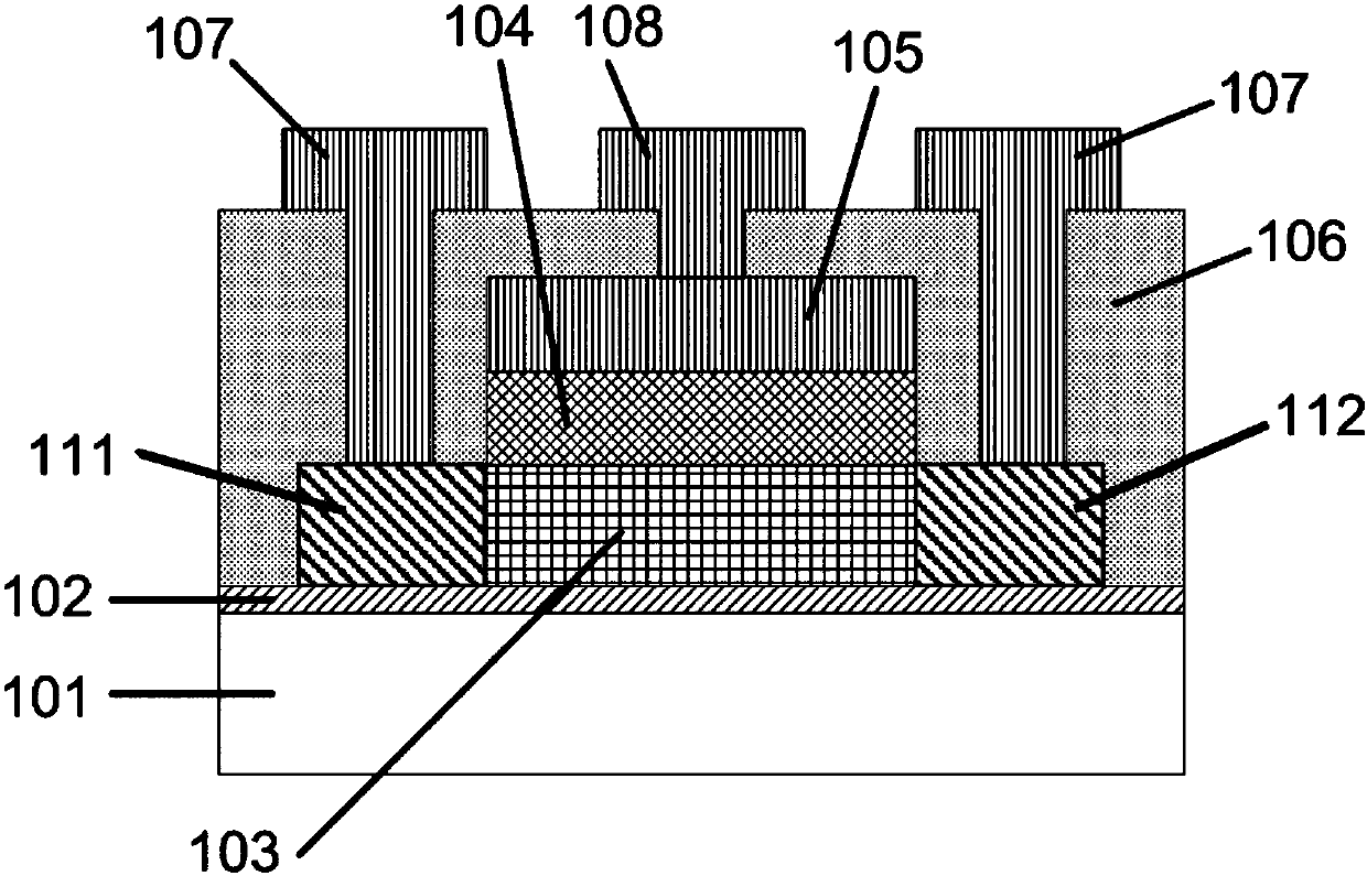
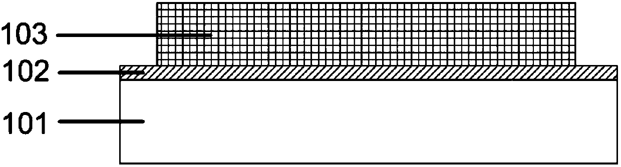
[0061] refer to figure 1 , an indium tin zinc oxide thin film transistor, comprising a substrate 101, the substrate 101 is provided with a buffer layer 102 composed of silicon dioxide, and the buffer layer 102 is provided with an indium tin zinc oxide thin film 103, The indium tin zinc oxide film 103 includes two low-resistance source-drain regions (the first low-resistance source-drain region 111 and the second low-resistance source-drain region 112) and a high-resistance channel region, and the indium tin zinc oxide A gate dielectric layer 104 composed of silicon dioxide is also provided on the object film 103, a conductive film 105 composed of metal aluminum is provided on the gate dielectric layer 104, and a conductive film 105 composed of metal aluminum is provided on the conductive film 105. The passivation layer 106 of silicon, the parts of the conductive film 105 and the indium tin zinc oxide film 103 not covered by the gate dielectric layer 104 are all covered by the ...

Embodiment 2

[0064] refer to Figure 1 to Figure 7 , a method for manufacturing a self-aligned top gate indium tin zinc oxide thin film transistor, comprising the following steps:

[0065] S1. Deposit a buffer layer 102 on a substrate 101 using a thermal oxidation growth method, such as figure 2 shown;

[0066] S2, on the buffer layer 102, use the magnetron sputtering method to deposit the indium tin zinc oxide film 103, such as image 3 As shown, the magnetron sputtering method is DC magnetron sputtering method and RF radio frequency magnetron sputtering method, and the targets used in the magnetron sputtering method are ITO targets and ZnO targets, wherein, Use a DC power supply when sputtering the ITO target, and the input power of the DC power supply is 120W; use a radio frequency power supply when sputtering the ZnO target material, and the input power of the radio frequency power supply is 150W; the reaction atmosphere is oxygen and argon, and the working pressure is 3 milliTorr ...


PUM


Abstract

The invention discloses a self-aligned top gate indium-tin-zinc oxide thin film transistor and a manufacturing method thereof. The transistor comprises a substrate, a buffer layer, an indium-tin-zincoxide thin film, a gate dielectric layer, a conductive thin film, a passivation layer, a source-drain contact electrode and a gate electrode. By adopting a self-aligned top gate structure, the problems that a traditional bottom gate transistor is high in parasitic capacitance and low in scaling capacity are overcome; and different air sources and annealing conditions are utilized when the passivation layer and the gate dielectric layer are deposited, so that the indium-tin-zinc oxide thin film transistor is in contact with the gate dielectric layer and an indium-tin-zinc oxide thin film area covered with the indium-tin-zinc oxide thin film transistor is in a high resistance state, the indium-tin-zinc oxide thin film transistor is in contact with the passivation layer and the indium-tin-zinc oxide thin film area covered with the indium-tin-zinc oxide thin film transistor is in a low resistance state, thereby forming a high-resistance channel region and a low-resistance source-drain region and solving the problem of the thermal stability of a traditional ion-doped metal oxide thin film transistor. The self-aligned top gate indium-tin-zinc oxide thin film transistor can be widely applied to the field of semiconductors.

Description

technical field [0001] The invention relates to the field of semiconductors, in particular to a self-aligned top gate indium tin zinc oxide thin film transistor and a manufacturing method thereof. Background technique [0002] Glossary: [0003] Precursor: It is the precursor or raw material for the synthesis of a substance. [0004] With the development and promotion of the next-generation new AMOLED active display, metal oxide thin film transistors have received more and more attention and research, among which bottom-gate indium tin zinc oxide thin film transistors (TFTs) are the most representative. However, the bottom-gate structure has the disadvantages of large parasitic capacitance and poor scaling capability, making it difficult to apply it to the integration of peripheral circuits to realize the system integration SOP of the display panel. A small number of scholars have carried out research on self-aligned top-gate structures with small parasitic capacitances. H...

Claims


Application Information

Patent Timeline
Patent Type & Authority Applications(China)
IPC IPC(8): H01L29/786H01L21/336
CPCH01L29/66969H01L29/7869H01L27/1225H01L27/1248H01L27/1251H01L27/127H01L21/02554
Inventor 陈荣盛邓孙斌郭海成
Owner SOUTH CHINA UNIV OF TECH
Why Eureka
Try Eureka