A self-aligned top-gate indium tin zinc oxide thin film transistor and its manufacturing method

一种氧化物薄膜、栅铟锡锌的技术,应用在晶体管、半导体/固态器件制造、半导体器件等方向,能够解决等比例缩小能力差、增加生产成本、器件短路等问题,达到等比例缩小能力强、生产成本降低、省去工艺步骤的效果

Active Publication Date: 2019-10-11
SOUTH CHINA UNIV OF TECH
View PDF4 Cites 0 Cited by
  • Summary
  • Abstract
  • Description
  • Claims
  • Application Information

AI Technical Summary

Problems solved by technology

However, the bottom-gate structure has the disadvantages of large parasitic capacitance and poor scaling capability, making it difficult to apply to the integration of peripheral circuits to realize the system integration SOP of the display panel.
A small number of scholars have carried out research on self-aligned top-gate structures with small parasitic capacitances. However, in the method of source-drain doping, hydrogen is generally used (J.Park et.al, Appl.Phys.Lett., 93, 053501 , 2008) or argon (B.DuAhn et.al, Appl.Phys.Lett., 93, 203506, 2008) plasma treatment to form a highly conductive region, since dopant ions easily diffuse from the source and drain regions to the channel, making The channel becomes low resistance, and the device is short-circuited. As long as a slight heat treatment is performed, the carrier concentration will change significantly, resulting in a sharp decline in device performance. Therefore, thin-film transistors that form high-conductivity regions by doping ions have thermal stability. Poor problem; and the formation of highly conductive regions by doping ions requires additional process steps, increasing production costs

Method used


Image

  • A self-aligned top-gate indium tin zinc oxide thin film transistor and its manufacturing method
  • A self-aligned top-gate indium tin zinc oxide thin film transistor and its manufacturing method
  • A self-aligned top-gate indium tin zinc oxide thin film transistor and its manufacturing method

Examples


Embodiment 1

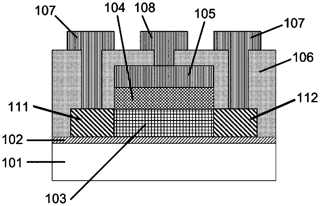
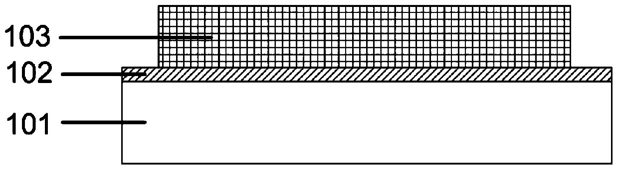
[0061] Reference figure 1 , An indium tin zinc oxide thin film transistor, comprising a substrate 101 on which a buffer layer 102 composed of silicon dioxide is provided, and an indium tin zinc oxide film 103 is provided on the buffer layer 102, The indium tin zinc oxide film 103 includes two low resistance source and drain regions (a first low resistance source and drain region 111 and a second low resistance source and drain region 112) and a high resistance channel region. The material film 103 is also provided with a gate dielectric layer 104 composed of silicon dioxide, the gate dielectric layer 104 is also provided with a conductive film 105 composed of metal aluminum, and the conductive film 105 is also provided with a composition of silicon dioxide. The passivation layer 106 of silicon, the conductive film 105 and the part of the indium tin zinc oxide film 103 that are not covered by the gate dielectric layer 104 are all covered by the passivation layer 106, and the pass...

Embodiment 2

[0064] Reference Figure 1 to Figure 7 , A manufacturing method of a self-aligned top gate indium tin zinc oxide thin film transistor, comprising the following steps:

[0065] S1. Use a thermal oxidation growth method to deposit a buffer layer 102 on the substrate 101, such as figure 2 Shown

[0066] S2. Use magnetron sputtering to deposit an indium tin zinc oxide film 103 on the buffer layer 102, such as image 3 As shown, the magnetron sputtering method is a DC DC magnetron sputtering method and an RF radio frequency magnetron sputtering method, and the target materials used in the magnetron sputtering method are an ITO target material and a ZnO target material, wherein, When sputtering ITO targets, use a DC power supply, the input power of the DC power supply is 120W; when sputtering ZnO targets, use a radio frequency power supply, the input power of the RF power supply is 150W; the reaction atmosphere is oxygen and argon, working pressure 3 millitorr (mTorr);

[0067] S3, perfo...


PUM

PropertyMeasurementUnit
poweraaaaaaaaaa

Abstract

The invention discloses a self-aligned top gate indium tin zinc oxide thin film transistor and a manufacturing method thereof. The transistor comprises a substrate, a buffer layer, an indium tin zinc oxide thin film, a gate dielectric layer, a conductive thin film, a passivation layer, a source drain contact electrode and gate electrode. The present invention adopts a self-aligned top-gate structure, which overcomes the problems of large parasitic capacitance and weak proportional reduction ability in traditional bottom-gate transistors, and uses different gas sources and annealing conditions when depositing passivation layers and depositing gate dielectric layers, so that The region of the indium tin zinc oxide film that is in contact with and covered by the gate dielectric layer presents a high resistance state, and the region of the indium tin zinc oxide film that is in contact with and covered by the passivation layer presents a low resistance state, thus forming a high resistance state. The channel region and the low-resistance source-drain region solve the thermal stability problem of the traditional metal oxide thin film transistor doped with ions. The invention can be widely used in the semiconductor field.

Description

Technical field [0001] The invention relates to the field of semiconductors, in particular to a self-aligned top gate indium tin zinc oxide thin film transistor and a manufacturing method thereof. Background technique [0002] Glossary: [0003] Precursor: It is the precursor or raw material for the synthesis of a substance. [0004] With the development and promotion of the next generation of new AMOLED active displays, metal oxide thin film transistors have received more and more attention and research, among which bottom gate indium tin zinc oxide thin film transistors (TFT) are the most representative. However, the bottom-gate structure has the shortcomings of large parasitic capacitance and poor scaling capability, so it is difficult to be applied to the integration of peripheral circuits to realize the system integration SOP of the display panel. A small number of scholars have carried out research on self-aligned top gate structures with small parasitic capacitance. However,...

Claims


Application Information

Patent Timeline
Patent Type & Authority Patents(China)
IPC IPC(8): H01L29/786H01L21/336
CPCH01L29/66969H01L29/7869H01L27/1225H01L27/1248H01L27/1251H01L27/127H01L21/02554
Inventor 陈荣盛邓孙斌郭海成
Owner SOUTH CHINA UNIV OF TECH
Why Eureka
Try Eureka