

Method for manufacturing different directions of surface metal circuits on small insulator
A technology for metal circuits and manufacturing methods, which is applied in the direction of removing conductive materials by chemical/electrolytic methods to achieve the effects of increasing usable area, reducing time, and improving finish
- Summary
- Abstract
- Description
- Claims
- Application Information
AI Technical Summary
Problems solved by technology
Method used
Image

Examples
Embodiment 1
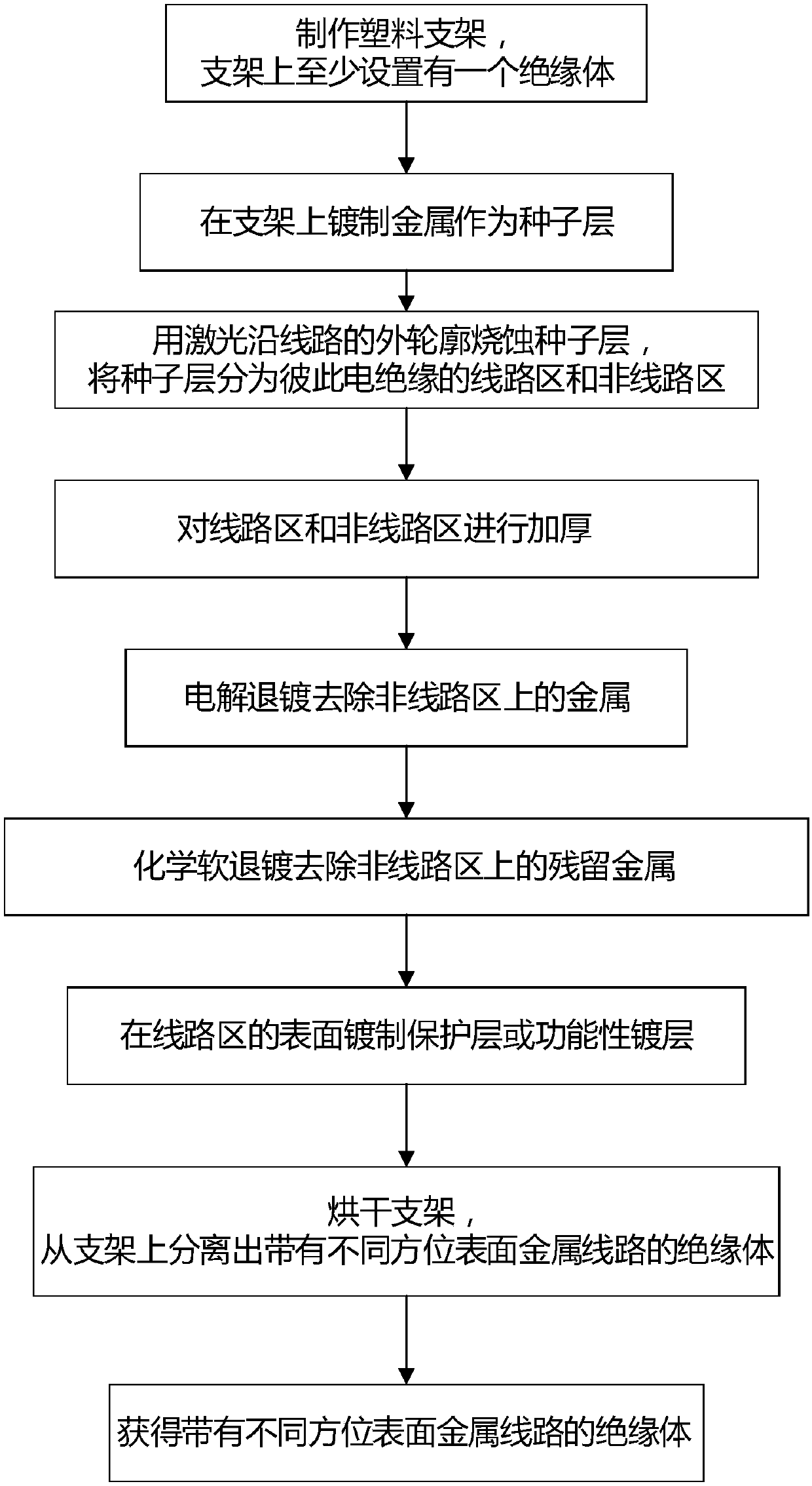
[0052] see figure 1 , the metal circuit manufacturing method on the surface of different orientations on the small insulator of the present invention comprises:
[0053] Step 1: Make a plastic bracket, and at least one insulator is arranged on the bracket;
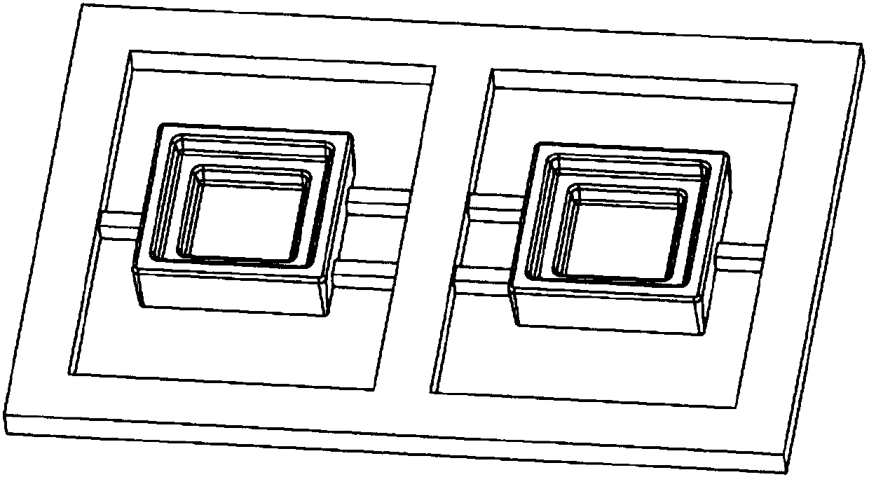
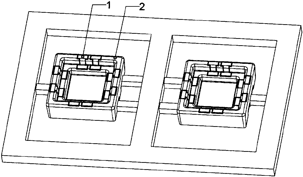
[0054] The bracket can be a plastic bracket or a metal bracket. If a plastic bracket is selected, the bracket can be made by injection molding. In this embodiment 1, a plastic insulator is used as an example. Of course, brackets of other materials can also be used. Be specific. The color of the bracket is preferably white. When making, first make the bracket connecting the insulator according to the size of the insulator, at least one insulator is arranged in the bracket, the periphery of the insulator is provided with a frame, and the insulator is arranged on the bracket through the frame, therefore, the number of insulators on the bracket can be configured as required, See figure 2 , in order to facilitate the produ...
Embodiment 2
[0068] This embodiment provides a method for manufacturing metal circuits on different orientation surfaces on a small insulator. Different from the plastic insulator in Embodiment 1, the bracket in this embodiment is made of metal. For the specific manufacturing method, see Figure 6 , now cooperate Figure 6 The manufacturing method is explained:
[0069] Step 1: making a metal bracket, at least one insulator is arranged on the bracket;
[0070] When making, first make the metal bracket connecting the insulator according to the size of the insulator. The metal bracket is formed by die-casting or forging or CNC, and then electrostatically sprays plastic on the surface to form a metal bracket. The color of the bracket is preferably white. At least one insulator is arranged in the bracket, and the periphery of the insulator is provided with a frame. The insulator is arranged on the bracket through the frame. Therefore, the number of insulators on the bracket can be configured...
Embodiment 3
[0079] On the basis of Embodiment 1, the present invention also provides a metal circuit manufacturing method on a small insulator with different orientation surfaces, see Figure 7 , now take the plastic insulator as an example to illustrate:
[0080] Step 1: making a bracket, at least one insulator is arranged on the bracket;
[0081] The bracket can be a plastic bracket or a metal bracket. For example, it can be made of a plastic bracket by injection molding, or a metal bracket connected to the insulator can be made according to the size of the insulator. The metal bracket can be molded by die-casting or forging or CNC, and then the plastic is electrostatically sprayed on the surface , thus forming a metal stent. Of course, brackets made of other materials may also be used, which is not specifically limited here. When making the bracket, first make the bracket connecting the insulator according to the size of the insulator. At least one insulator is arranged in the bracke...
PUM
 Abstract
Description
Claims
Application Information