

Patterned bank structures on substrates and methods of formation
A substrate and bank technology, applied to the patterned bank structure and formation field on the substrate, can solve the problems of increased thickness unevenness and the contact angle cannot be too low
- Summary
- Abstract
- Description
- Claims
- Application Information
AI Technical Summary
Problems solved by technology
Method used
Image

Examples
other Embodiment approach
[0082] Other embodiments may include fabrication of organic electronic (OE) devices, such as top-gate or bottom-gate organic field-effect transistors (OFETs), including organic thin-film transistors (OTFTs), organic light-emitting diodes (OLEDs), or organic photovoltaic (OPV) devices, including solar cells and photoelectric sensors).
[0083] Embodiments of the invention also include products or assemblies comprising organic electronic devices as described above and below. Such products or components are integrated circuits (ICs), radio frequency identification (RFID) tags, security tags or security devices incorporating RFID tags, flat panel displays (FPDs), backplanes for FPDs, backlights for FPDs, electrowetting devices, electronic Photographic devices, electrophoretic devices, electrophotographic recording devices, organic memory devices, sensors, biosensors or biochips. The present invention also relates to a method of preparing an organic electronic device, such as a to...
Embodiment 1
[0091] A commercially available cresol novolac resin mixture CNR1 (10 parts; composition described below) and fluorinated materials A, B, C, and D (1 part) in a resin:fluorinated material weight ratio of 2.3:1 The resist formulation was spin-coated at a thickness of 2 μm on a 50 nm thick ITO layer on a glass substrate. The photoresist was soft baked on a hot plate at 90 to 100° C. for 2 minutes to remove the solvent. Then, using a mask aligner, the photoresist was exposed using a photomask using 365 nm ultraviolet light. The exposed samples were developed in 2.5% TMAH aqueous solution, followed by rinsing several times with deionized water, then blow-dried and hard baked on a hot plate at 130 to 180 °C for 1 to 30 minutes.
[0092] CNR1 contains 23% cresol novolac resin, 3% 2-diazo-1-naphthoquinone sulfonate (DNQ of the present invention) of 2,3,4-trihydroxybenzophenone, 1% 2 , 6-bis(hydroxymethyl)-p-cresol crosslinker, 0.01% silicone dispersant and 73% 1-methoxy-2-propyl ac...
Embodiment 2
[0100] Using the same procedure as in Example 1, using the same mixture of cresol novolac resins and fluorosurfactant D of the present invention in the specified weight ratios, and using different thermal conditions, photoresist formulations were prepared. Measuring the contact angle of embankment to water (CA H2O ) and the contact angle of ITO substrate to 3-phenoxytoluene (CA 3PT ) and are shown in Table 2.
[0101] Table 2 - Contact angles for Experiment 2
[0102]
[0103]
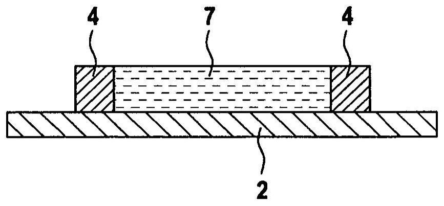
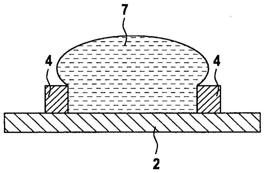
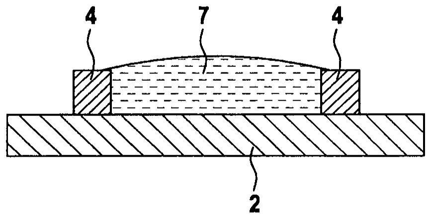
[0104] Note that in Table 2, the ratio of resin:fluorosurfactant of the present invention is greater than 2:1, ideally below 10:1, more ideally below 7:1, in order to obtain the non-wetting properties of the bank structure. Bigger improvements. This is particularly desirable when the active material is introduced into the trap from an aqueous solution. After the photoresist process, the wetting properties of the ITO substrates improved and most of the improvement was preserved in the presence...
PUM
| Property | Measurement | Unit |
|---|---|---|
| height | aaaaa | aaaaa |
| height | aaaaa | aaaaa |
| thickness | aaaaa | aaaaa |
Abstract
Description
Claims
Application Information