A method of winding compensation in via holes

A wire winding and hole wall technology, which is applied in the direction of electrical connection of printed components, printed circuit components, printed circuits, etc., can solve the problems of limited parts and wiring space, sacrifice of layout and wiring space, and unfavorable parts and signal layout and wiring, etc. , to improve space utilization, reduce signal transmission delay, and optimize board performance

Active Publication Date: 2020-01-31
SUZHOU METABRAIN INTELLIGENT TECH CO LTD
View PDF6 Cites 0 Cited by
  • Summary
  • Abstract
  • Description
  • Claims
  • Application Information

AI Technical Summary

Problems solved by technology

[0005] 1) A large amount of board space is occupied for winding compensation, which is not conducive to the layout and wiring of other parts and signals
[0006] 2) Sacrifice the layout and wiring space of other parts or signals, which will affect the overall performance of the board
[0007] Moreover, on a certain PCB board size, there are more and more functions to be realized, and the space for parts and wiring is becoming more and more limited. How to improve the space utilization of the board has become a key issue

Method used


Image

  • A method of winding compensation in via holes
  • A method of winding compensation in via holes
  • A method of winding compensation in via holes

Examples


Embodiment 1

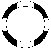
[0030] like figure 2 As shown, it is an ordinary via hole on the PCB, the inner ring is a drill hole, and the black circle means that the copper ring runs through the PCB board up and down, and has conductive properties.

[0031] like image 3 , 4 As shown, a method of winding compensation in the via through hole, in the design of the PCB board, uses the via through hole that penetrates up and down in the PCB board, and wires are routed up and down the hole wall to perform winding compensation, reducing the winding on the board surface. Line space, so as to achieve the purpose of improving the utilization rate of the board and optimizing the performance of the board.

Embodiment 2

[0033] On the basis of embodiment 1, the implementation steps of the method described in this embodiment include:

[0034] Select the signal via hole that needs winding compensation, and perform up and down winding in the through hole;

[0035] During the production of the PCB board factory, the copper wires wound up and down in the via holes are corroded and developed.

Embodiment 3

[0037] On the basis of embodiment 1 or 2, the implementation steps of the method described in this embodiment also include:

[0038] Fill the via hole with resin to protect the copper wire in the hole.


PUM


Abstract

The invention discloses a novel method for winding compensation in a via through hole. In design of a printed circuit board (PCB) card, winding compensation is performed by vertical wiring on a hole wall of the via through hole vertically penetrating through a PCB. The via through hole vertically penetrating through the PCB is utilized, signal winding compensation is performed in the via through hole, signal transmission delay on the PCB is reduced, meanwhile, the space utilization of a PCB panel is improved, and the board card performance is optimized.

Description

technical field [0001] The invention relates to the technical field of server board design, in particular to a method for compensating wire winding in via through holes. Background technique [0002] With the rapid development of the server industry, the performance of server boards is increasing. In order to improve the reliability of server products, the industry has higher and higher requirements for signals in PCB boards. [0003] In order to reduce the transmission delay of the signal on the PCB board and improve the transmission quality of the signal, it usually takes up a lot of space on the board to perform winding compensation to achieve signal length matching (such as figure 1 ). [0004] However, the method of winding compensation will bring the following disadvantages: [0005] 1) A large amount of board space is occupied for winding compensation, which is not conducive to the layout and wiring of other parts and signals. [0006] 2) Sacrificing the layout an...

Claims


Application Information

Patent Timeline
Patent Type & Authority Patents(China)
IPC IPC(8): H05K1/11H05K3/40
CPCH05K1/11H05K3/4038H05K2201/09281
Inventor 王英娜
Owner SUZHOU METABRAIN INTELLIGENT TECH CO LTD
Why Eureka
Try Eureka