A method for reorganizing nand-flash chip data

A data and chip technology, which is applied in the field of reorganizing NAND-Flash chip data, can solve the problems of low recovery and recombination efficiency, cumbersome and complicated operations, and achieve data recovery and electronic forensics. The method is simple and effective, and the recovery and recombination are successful. high rate effect

Active Publication Date: 2021-08-27
SICHUAN QIAODUOTIANGONG PRECISION EQUIP CO LTD
View PDF5 Cites 0 Cited by
  • Summary
  • Abstract
  • Description
  • Claims
  • Application Information

AI Technical Summary

Problems solved by technology

In the prior art, there are few effective recovery and reorganization methods for the failure of NAND-Flash storage devices. Some recovery and reorganization technical solutions are too complicated, cumbersome to operate, and the recovery and reorganization efficiency is low, especially for NAND -The recovery and reorganization of the main control chip model of the Flash chip is SSS6677, and there is no specific technical solution in the prior art

Method used


Image

  • A method for reorganizing nand-flash chip data
  • A method for reorganizing nand-flash chip data
  • A method for reorganizing nand-flash chip data

Examples


Embodiment Construction

[0035] The present invention will be further elaborated below in conjunction with the accompanying drawings and embodiments.

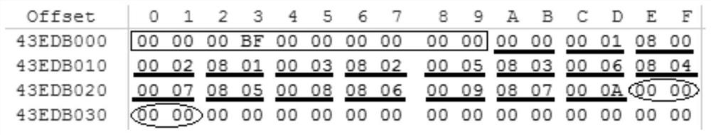
[0036] In this embodiment, the U disk of the NAND-Flash chip whose main control chip model is selected as SSS6677 is used as the storage device for data reorganization. The U disk is composed of multiple physical blocks, and each physical block is composed of 0x80 pages. Each page Have the same page structure and the byte length is 0x10E0, each page consists of 8 sectors, 8 management areas and a padding area, the byte length of each sector is 0x200, the byte length of each management area is 0x10, and the byte length of the padding area is 0x60; therefore, the byte length of each physical block is 0x10E0*0x80, that is, 0x87000.

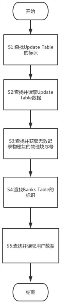
[0037] like figure 1 Shown, a method for reorganizing NAND-Flash chip data, comprises the following steps:

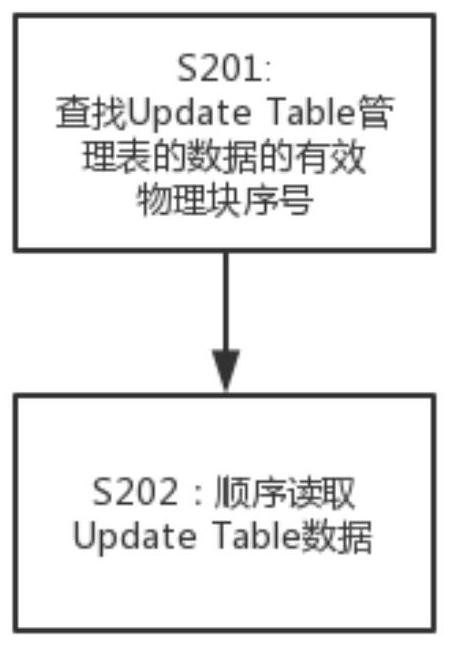
[0038] S1: within the range of byte length 0x87000 of each physical block of the U disk, with the first byte addre...


PUM


Abstract

The invention discloses a method for reorganizing NAND-Flash chip data, which is characterized in that it includes the following steps, S1: within the byte length range of each physical block of the NAND-Flash chip, use the header of each physical block Byte address is initial address, searches for the mark of Update Table; S2: according to the mark of described Update Table, finds and reads Update Table data; S3: finds and obtains the physical of the invalid record physical block of described NAND-Flash chip Block sequence number, the invalid record physical block is a physical block that does not store data; S4: search for the logo of the Banks Table; S5: search and read user data according to the logo of the Banks Table; the present invention has simple and effective, data The beneficial effect of recovering and recombining high efficiency, and solving the problem that there is no data reorganizing technical solution for the chip whose main control chip model is SSS6677 in the prior art, realizes the data recovery of this type of NAND-Flash storage device and e-discovery.

Description

technical field [0001] The invention belongs to the field of data restoration and electronic evidence collection, and relates to data restoration and evidence collection of Flash chips, in particular to a method for recombining NAND-Flash chip data. Background technique [0002] NAND-Flash memory is a kind of Flash memory. It adopts nonlinear macro-cell mode inside, which provides a cheap and effective solution for the realization of solid-state large-capacity memory. NAND-Flash memory has the advantages of large capacity and fast rewriting speed, and is suitable for the storage of large amounts of data, so it has been more and more widely used in the industry. For example, embedded products include digital cameras, MP3 walkman memory cards, volume Small U disk, etc. [0003] However, when important data is stored in the NAND-Flash storage device and the NAND-Flash storage device fails and the user cannot read and write data normally, it is necessary to remove the memory ch...

Claims


Application Information

Patent Timeline
Patent Type & Authority Patents(China)
IPC IPC(8): G06F12/06
CPCG06F12/0646
Inventor 梁效宁许超明赵飞何升
Owner SICHUAN QIAODUOTIANGONG PRECISION EQUIP CO LTD
Why Eureka
Try Eureka