Pixel compensating circuit and driving method thereof, display panel and display apparatus

A compensation circuit and pixel technology, applied to static indicators, instruments, etc., can solve problems such as long charging time, insufficient threshold compensation, and small charging current

Active Publication Date: 2018-04-20
HEFEI BOE OPTOELECTRONICS TECH +1
View PDF7 Cites 21 Cited by
  • Summary
  • Abstract
  • Description
  • Claims
  • Application Information

AI Technical Summary

Problems solved by technology

However, when the written data signal is a low-gray-scale data signal, the charging current of the low-gray-scale data signal is small, resu...

Method used


Image

  • Pixel compensating circuit and driving method thereof, display panel and display apparatus
  • Pixel compensating circuit and driving method thereof, display panel and display apparatus
  • Pixel compensating circuit and driving method thereof, display panel and display apparatus

Examples


Embodiment 1

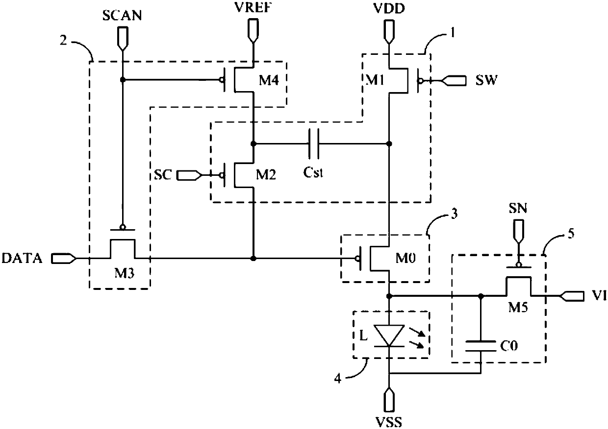
[0081] by Figure 2b The structure of the pixel compensation circuit shown is taken as an example, and the corresponding circuit timing diagram is as follows Figure 4a shown. Specifically, choose the Figure 4a There are three stages in the timing diagram shown: reset stage T1 , threshold compensation stage T2 and light emitting stage T3 .

[0082] In the reset phase T1, SCAN=0, SC=1, SW=0, SN=0. Since SCAN=0, both the third switch transistor M3 and the fourth switch transistor M4 are turned on. The turned-on third switch transistor M3 inputs the data signal of the data signal terminal DATA into the control electrode of the driving transistor M0, so that the voltage of the control electrode of the driving transistor M0 is the voltage V of the data signal. data . The turned-on fourth switching transistor M4 transmits the signal of the reference voltage signal terminal VREF to the second terminal of the storage capacitor Cst, so that the voltage of the second terminal of t...

Embodiment 2

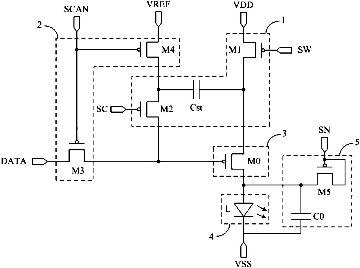
[0087] by Figure 3a The structure of the pixel compensation circuit shown as an example, Figure 3a The pixel compensation circuit shown is in the Figure 2b On the basis of the pixel compensation circuit shown, the signal of the scanning signal terminal SCAN is used to control the second switching transistor M2, and the second switching transistor M2 is an N-type transistor, and the third switching transistor M3 and the fourth switching transistor M4 are both P-type Transistor, its corresponding circuit timing diagram is as follows Figure 4b shown. Specifically, choose the Figure 4bThere are three stages in the timing diagram shown: reset stage T1 , threshold compensation stage T2 and light emitting stage T3 .

[0088] In the reset phase T1, SCAN=0, SW=0, SN=0. In this stage, since SCAN=0, the second switching transistor M2 is turned off. The rest of the working process in this stage is basically the same as the working process in the reset stage T1 in the first embo...

Embodiment 3

[0092] by Figure 3b The structure of the pixel compensation circuit shown as an example, Figure 3b The pixel compensation circuit shown is in the Figure 3a On the basis of the pixel compensation circuit shown, the second switch transistor M2 is a P-type transistor, the third switch transistor M3 and the fourth switch transistor M4 are both N-type transistors, and the corresponding circuit timing diagram is as follows Figure 4c shown. Specifically, choose the Figure 4c There are three stages in the timing diagram shown: reset stage T1 , threshold compensation stage T2 and light emitting stage T3 .

[0093] In the reset phase T1, SCAN=1, SW=0, SN=0. In this stage, since SCAN=1, both the third switch transistor M3 and the fourth switch transistor M4 are turned on, and the second switch transistor M2 is turned off. The rest of the working process in this stage is basically the same as the working process in the reset stage T1 in the first embodiment, and will not be desc...


PUM


Abstract

The invention discloses a pixel compensating circuit and a driving method thereof, a display panel and a display apparatus. The pixel compensating circuit comprises a control module, a write-in module, a driving module, a light-emitting module and a resetting module; data signals of a data signal terminal are transmitted to the driving module through the write-in module under the control of a scanning signal terminal, and signals of a reference voltage signal terminal are transmitted to the control module; the control module transmits signals of a first power supply terminal to the driving module under the control of a power supply control signal terminal; and the control module controls the driving module to perform discharging for threshold compensation under the common effect of a switch-on control signal terminal and the power supply control signal terminal to write a threshold voltage of a driving transistor in the driving module. According to the system, the pixel compensating circuit is charged by employing the signals of the first power supply terminal so that the threshold voltage of the driving transistor can be rapidly written in, the compensation charging time is reduced, and the stability of light-emitting display is improved; and the light-emitting module is reset through the resetting module so that the problem of reduced performance and service lifetime can be improved.

Description

technical field [0001] The invention relates to the field of display technology, in particular to a pixel compensation circuit, a driving method thereof, a display panel and a display device. Background technique [0002] Organic Light-Emitting Diode (OLED) is one of the hotspots in the field of flat panel display research today. Compared with Liquid Crystal Display (LCD), OLED has fast response, high brightness, high contrast, and low power consumption. As well as the advantages of easy realization of flexible display, it is considered to be the next generation mainstream display. Unlike LCD, which uses a stable voltage to control brightness, OLED is current-driven and requires a stable current to control light emission. At present, it is generally set in an OLED display that can compensate the threshold voltage V of the driving transistor th The pixel compensation circuit is used to drive the OLED to emit light, and the charging is performed by writing the data signal in...

Claims


Application Information

Patent Timeline
IPC IPC(8): G09G3/3225
CPCG09G3/3225G09G2300/0852G09G2300/0861G09G2310/0251G09G2310/0262G09G3/3233G09G2320/043G09G2330/021G09G2320/0233
Inventor 凌杰王文坚张斗庆
Owner HEFEI BOE OPTOELECTRONICS TECH
Why Eureka
Try Eureka