Connection method and connection structure of radio frequency PCB

A connection structure and connection method technology, applied in the field of electronics, can solve problems such as difficulty in meeting the requirements of RF PCB connection impedance control, and achieve the effects of facilitating observation of welding effects, good impedance control and grounding, and good mechanical energy.

Pending Publication Date: 2018-04-20
COMBA TELECOM SYST CHINA LTD
View PDF0 Cites 2 Cited by
  • Summary
  • Abstract
  • Description
  • Claims
  • Application Information

AI Technical Summary

Problems solved by technology

[0004] The existing technology can use the exposed copper contact between the PCB boards to realize the connection of two RF PCBs, but this method is difficult to meet the impedance control requirements in the RF PCB connection

Method used


Image

  • Connection method and connection structure of radio frequency PCB
  • Connection method and connection structure of radio frequency PCB
  • Connection method and connection structure of radio frequency PCB

Examples


Embodiment Construction

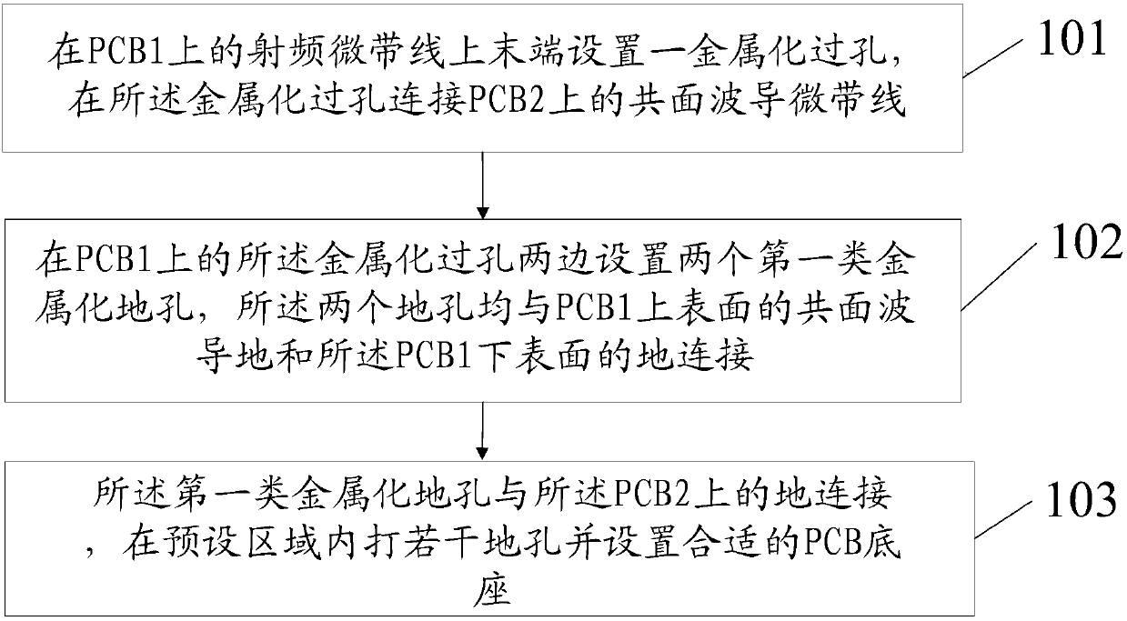
[0034] The present invention provides a connection method and a connection structure of a radio frequency PCB, which are used to solve the problem in the prior art that it is difficult to realize the high performance connection of the radio frequency PCB at a low cost.

[0035] In order to solve the above technical problem, the general idea of ​​the technical solution in the embodiment of the present invention is as follows: a good magnetic field loop is formed around the connection of the radio frequency microstrip line, so that the insertion loss and standing wave of the connection line are better in a wide frequency band.

[0036] A connection method is provided, and the specific implementation steps are as follows:

[0037] Please refer to figure 1 As shown, it is a flowchart of a connection method provided by an embodiment of the present invention. The method includes:

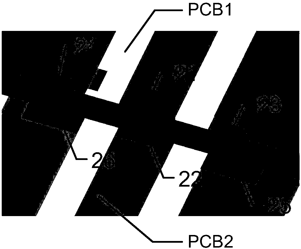
[0038] Step 101 : a metallized via hole is arranged at the end of the radio frequency microstrip lin...


PUM


Abstract

The present invention proposes a connection method and a connection structure of a radio frequency PCB. A metalized via of the appropriate size is designed at the end of a PCB1 radio frequency microstrip line. One end of the metalized via is connected to the end of a radio frequency microstrip transmission line on the PCB1, and the other end is connected to a first signal pad on the lower surfaceof the PCB1. There is also a second signal pad on a PCB2 at a position corresponding to the first signal pad of the PCB1. The PCB1 and the PCB2 are soldered together by two pads. Both the PCB1 and PCB2 on both sides of a radio frequency microstrip via are provided with ground pads soldered together. With the technical scheme of the present invention, the two connected PCBs can be grounded with good standing wave, and the beneficial effect of small insertion loss can be achieved.

Description

technical field [0001] The invention relates to the field of electronic technology, in particular to a connection method and a connection structure of a radio frequency PCB. Background technique [0002] With the rapid development of mobile communications, especially the development of 4G communications, there are more and more demands for serialization and platformization of electronic products. In serialized products, modularizing circuits with the same function will effectively reduce the development cycle. cost. This design concept is also applicable to RF circuits. The use of sub-board design for RF circuits will be more conducive to reducing costs, obtaining better performance, and serializing platforms. For example, if the power amplifier uses rogers plates alone, the cost is lower than that of mixed pressure; if the same specifications are different The devices of the frequency band can be modularized to the frequency-related devices, that is, a single PCB. [0003...

Claims


Application Information

Patent Timeline
Patent Type & Authority Applications(China)
IPC IPC(8): H05K1/02H05K1/11
CPCH05K1/0218H05K1/0237H05K1/0251H05K1/116H05K1/117H05K2201/09563
Inventor 范莉张志梅朱艳涛罗成庆
Owner COMBA TELECOM SYST CHINA LTD
Why Eureka
Try Eureka