Packaging structure and manufacturing method thereof

A technology of packaging structure and manufacturing method, which is applied in semiconductor/solid-state device manufacturing, electrical components, electrical solid-state devices, etc., can solve the problems of thin package thickness and volume, electromagnetic wave interference, etc., achieve thin package thickness and volume, and avoid electromagnetic wave interference. Effect

Active Publication Date: 2018-05-01
UNIMICRON TECH CORP
View PDF3 Cites 1 Cited by
  • Summary
  • Abstract
  • Description
  • Claims
  • Application Information

AI Technical Summary

Problems solved by technology

[0004] The present invention provides a packaging structure, the active surfaces of two adjacent electronic components face opposite directions respectively, and the piezoelectric cooling unit is arranged in the opening of the layered circuit structure, which can effectively solve the problem of existing electronic components. The problem of electromagnetic interference, and can have a thinner package thickness and volume, in line with today's demand for thinner products

Method used


Image

  • Packaging structure and manufacturing method thereof
  • Packaging structure and manufacturing method thereof
  • Packaging structure and manufacturing method thereof

Examples


Embodiment Construction

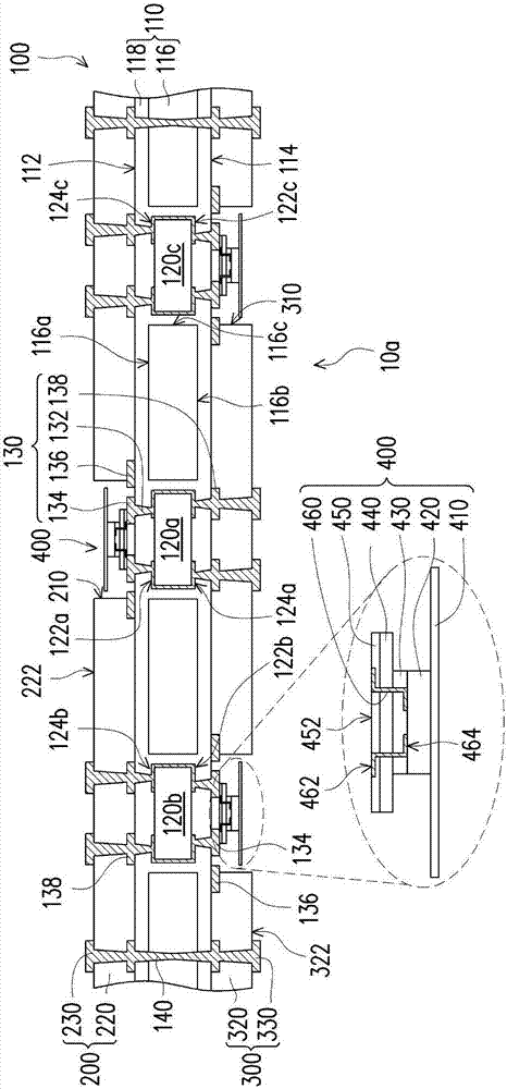
[0089] figure 1 A cross-sectional schematic diagram of a package structure according to an embodiment of the present invention is shown. Please refer to figure 1 In this embodiment, the package structure 10a includes a circuit substrate 100, a first build-up wiring structure 200, a second build-up wiring structure 300, and a plurality of piezoelectric heat dissipation units 400. The circuit substrate 100 includes a core layer 110, a plurality of electronic components ( figure 1 Three electronic components 120a, 120b, 120c) and a conducting unit 130 are schematically shown in FIG. The core layer 110 has a first surface 112 and a second surface 114 opposite to each other. The electronic components 120a, 120b, 120c are embedded in the core layer 110, and each of the electronic components 120a (or 120b, 120c) has an active surface 122a (or 122b, 122c) and a back surface 124a (or 124b, 124c), and the active surfaces 122a, 122b (or 122a, 122c) of two adjacent electronic components 1...


PUM


Abstract

The invention relates to a packaging structure and a manufacturing method thereof. The packaging structure comprises a circuit substrate, a first layer-adding line structure, a second layer-adding line structure, and a plurality of piezoelectric heat radiating units. The circuit substrate comprises a core layer, a plurality of electronic components, and a conducting unit. The electronic componentsare imbedded in the core layer, and the active surfaces of two adjacent electronic components respectively face towards the a first surface and a second surface of the core layer. The conducting unitis configured to the core layer and is electrically connected to the electronic components. The first and second layer-adding line structure are respectively configured to the first and second surface, and are respectively provided with at least one first opening and one second opening. Each piezoelectric heat radiating unit is corresponding to the active surface of the electronic component, andis electrically connected to the conducting unit, exposing from the first opening and the second opening. The invention is advantageous in that the electromagnetic wave interference among the electronic components can be prevented; the packaging is thin and volume can be small; the thin-type demand can be met.

Description

Technical field [0001] The present invention relates to a packaging structure and a manufacturing method thereof, and in particular to a packaging structure with heat dissipation function and a manufacturing method thereof. Background technique [0002] With the increasing development of the technology industry, electronic components in electronic products are also moving towards high-efficiency, high-speed and multi-functional development. However, these electronic components generate a large amount of heat energy during operation. Therefore, how to integrate the heat dissipation module design into the electronic device to reduce the working heat energy generated by the electronic components has become one of the urgent problems to be solved. [0003] In the existing packaging structure, the piezoelectric material is attached to the inside of the metal shielding cover, and the metal shielding cover is erected on the package carrier to define a containing cavity with the package ca...

Claims


Application Information

Patent Timeline
Patent Type & Authority Applications(China)
IPC IPC(8): H01L23/433H01L25/00H01L21/48
CPCH01L21/4882H01L23/4334H01L25/00
Inventor 黄祥纮
Owner UNIMICRON TECH CORP
Why Eureka
Try Eureka