Efficient method for quality tracing of multilayer PCB

A high-quality and high-efficiency technology, applied in the direction of collaborative equipment, instruments, computer parts, etc., can solve problems such as being susceptible to adverse effects, data loss and identification, etc., to reduce processing workload, ensure accurate identification, and improve work efficiency. Effect

Active Publication Date: 2018-05-04
GUANGDONG ZHENGYE TECH
View PDF5 Cites 14 Cited by
  • Summary
  • Abstract
  • Description
  • Claims
  • Application Information

AI Technical Summary

Problems solved by technology

[0007] The purpose of the present invention is to provide an efficient quality traceability method for multi-layer PCBs, which overcomes the defects that data is easily lost and identification is easily affected by adverse effects in the prior art when two-dimensional codes are used as traceability marks, and realizes two-dimensional codes to Conversion of hole matrix codes with fewer holes

Method used


Image

  • Efficient method for quality tracing of multilayer PCB
  • Efficient method for quality tracing of multilayer PCB
  • Efficient method for quality tracing of multilayer PCB

Examples


Embodiment Construction

[0050]In order to make the purpose, features and advantages of the present invention more obvious and understandable, the technical solutions in the embodiments of the present invention will be clearly and completely described below in conjunction with the accompanying drawings in the embodiments of the present invention. Obviously, the following The described embodiments are only some, not all, embodiments of the present invention. Based on the embodiments of the present invention, all other embodiments obtained by persons of ordinary skill in the art without making creative efforts belong to the protection scope of the present invention.
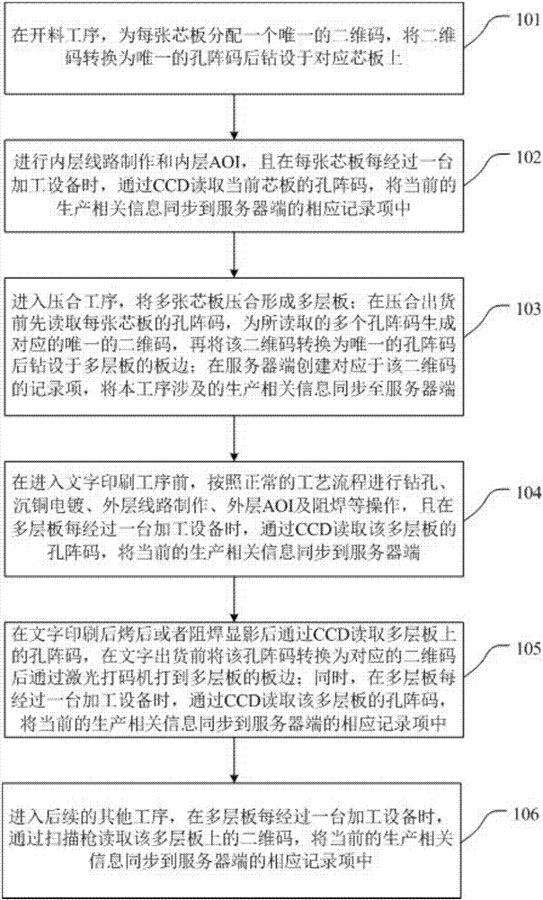
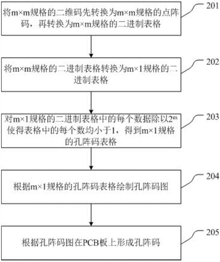
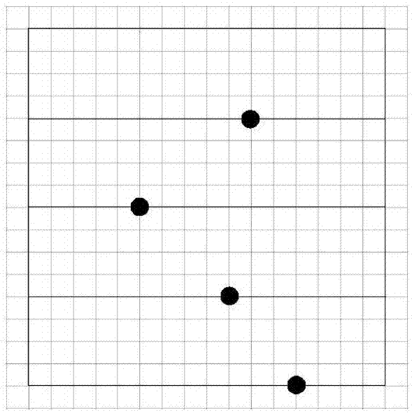
[0051] The core idea of ​​the present invention is: aiming at the defects of two-dimensional codes in certain processes, in the whole production process of multi-layer PCB, the corresponding two-dimensional codes are first generated for each core board, and the corresponding two-dimensional codes are generated from the cutting process to th...


PUM


Abstract

The invention discloses an efficient method for quality tracing of a multilayer PCB. The method includes the steps of distributing two-dimensional codes for each core plate in a cutting process, converting the two-dimensional codes into aperture array codes and drilling the aperture array codes in the corresponding core plates; in a press fit process, reading the aperture array codes on each coreplate, combining all the read aperture array codes to generate corresponding two-dimensional codes, and converting the corresponding two-dimensional codes into aperture array codes and then drilling the aperture array codes in the multilayer board; after a solder resist process, reading the aperture array codes on the multilayer board, and converting the aperture array codes into corresponding two-dimensional codes and drilling the two-dimensional codes in the multilayer board. A method for conversion from a two-dimensional code to an aperture array code includes the steps of converting the two-dimensional code into a binary form with a m * m specification, and dividing the binary form into at least two parts; converting each part into an aperture array code local graph; and combining allthe obtained aperture array code local graphs into a complete aperture array code graph, and finally forming the aperture array code on the PCB. According to the efficient method for quality tracing of the multilayer PCB, the two-dimensional code can be converted into the aperture array code with a smaller number of apertures, the processing workload is reduced, and it is effectively ensured thattracing markers are accurately identified.

Description

technical field [0001] The present invention relates to the technical field of PCB (Printed Circuit Board, printed circuit board), in particular to an efficient quality tracing method of multilayer PCB. Background technique [0002] Traceability of the cause of product problems is a serious challenge for manufacturers in every industry, from automotive to aerospace, from medical to food. In an era of globalization, businesses pursue relationship management to maximize customer satisfaction. Consumer and environmental regulations are becoming stricter, making traceability even more necessary. [0003] More than ever, manufacturers are looking to maximize production capacity and reduce costs. To achieve this goal, every step in the entire manufacturing process must be monitored and complete historical records kept. Issues affecting product quality must be quickly identified and corrected to prevent defective products from continuing down the production line, with the ultima...

Claims


Application Information

Patent Timeline
Patent Type & Authority Applications(China)
IPC IPC(8): G06K17/00
CPCG06K17/0022
Inventor 梅领亮廉世周赵冶蓝薇宋国营徐地华
Owner GUANGDONG ZHENGYE TECH
Why Eureka
Try Eureka