Semiconductor devices and methods of forming same

A semiconductor and device technology, applied in the field of forming through-substrate through-hole conductors, can solve problems such as multiple die areas, and achieve the effect of simplifying the process flow, fewer masks and process steps, and unlimited compactness and density

Inactive Publication Date: 2018-05-11
NANYANG TECH UNIV
View PDF12 Cites 11 Cited by
  • Summary
  • Abstract
  • Description
  • Claims
  • Application Information

AI Technical Summary

Problems solved by technology

Fabricating through-substrate vias and deep trench capacitors is challenging and expensive because they occupy significantly more die area than modern metal-oxide-semiconductor field-effect transistors (MOSFETs)

Method used


Image

  • Semiconductor devices and methods of forming same
  • Semiconductor devices and methods of forming same
  • Semiconductor devices and methods of forming same

Examples


Embodiment Construction

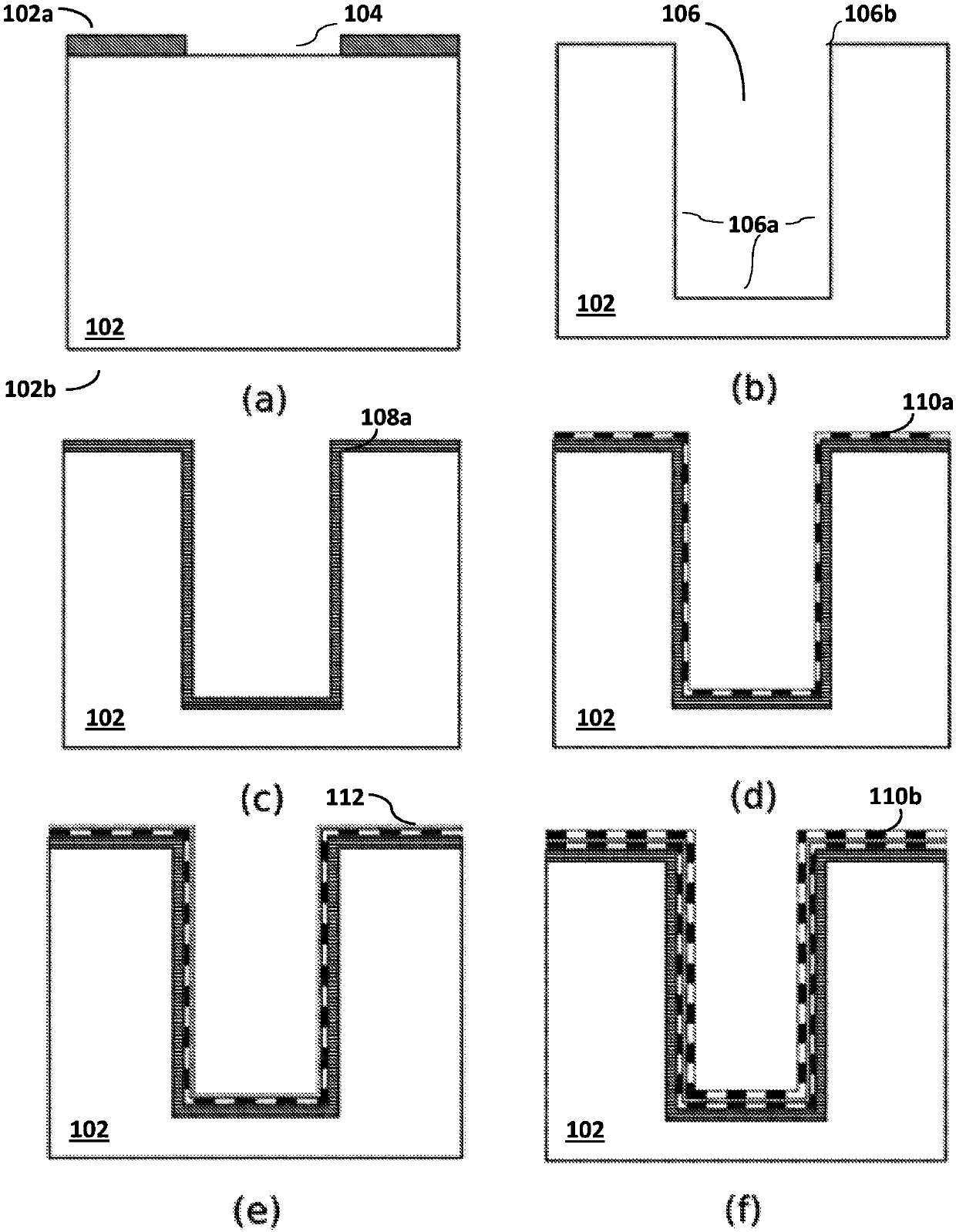
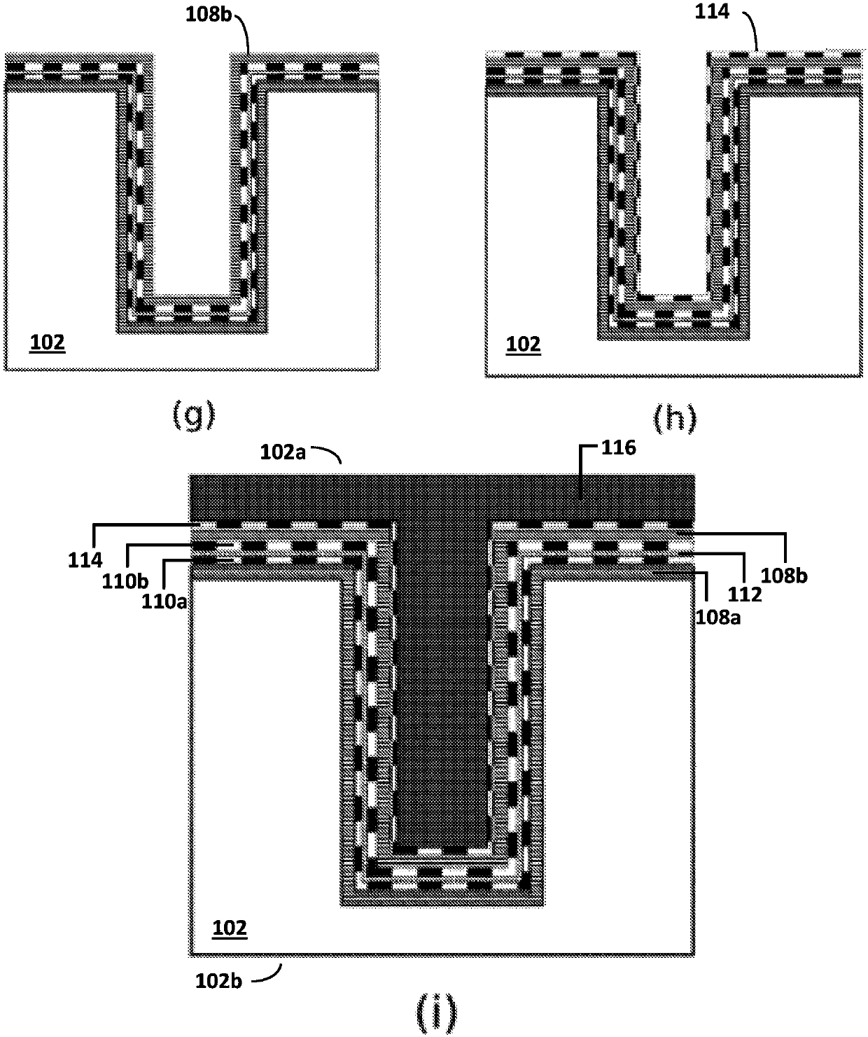
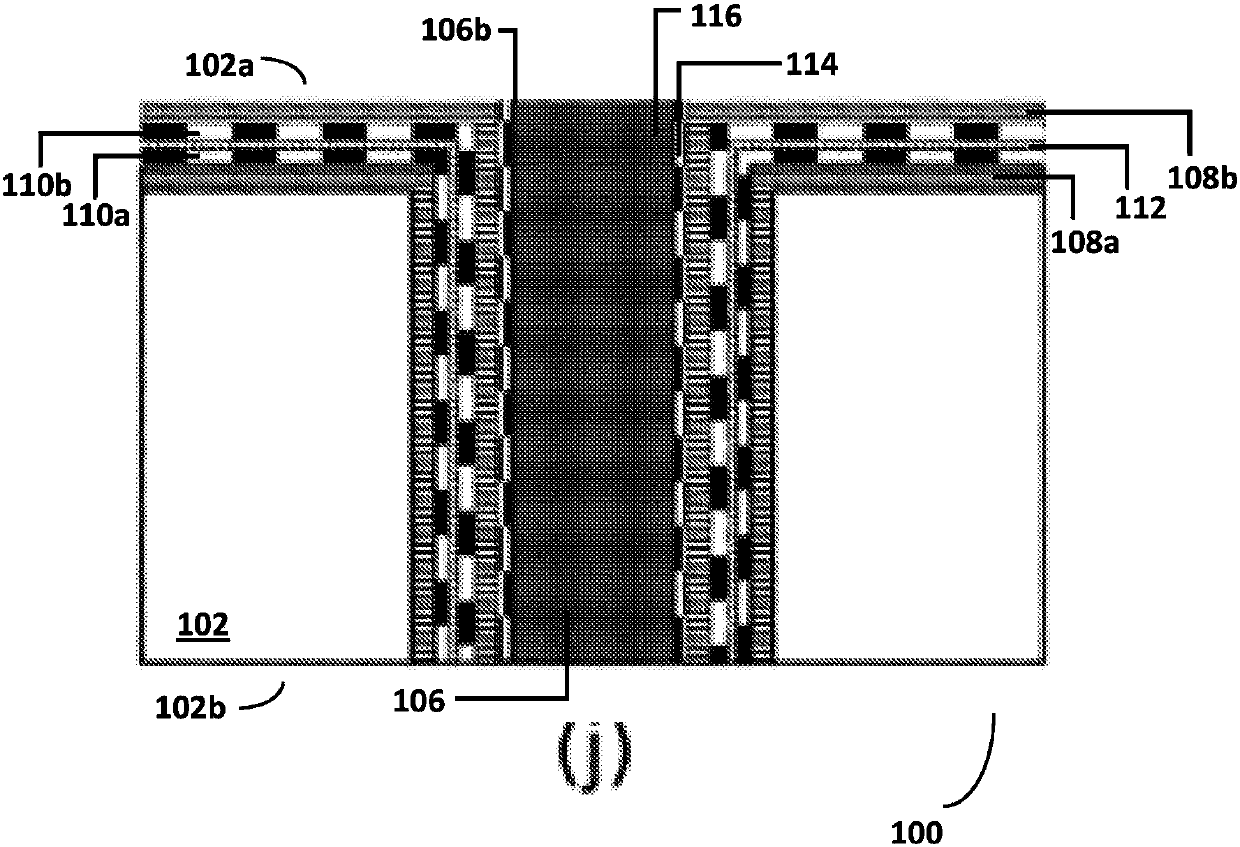
[0029] Now turning to the above mentioned figure 1 , which provides a series of figures illustrating an exemplary process flow for forming the first semiconductor device 100 . figure 1 (a) shows the substrate 102 having a first side 102a and a second side 102b. In at least one implementation, substrate 102 is at least partially formed of silicon. The window 104 is patterned from photoresist on the substrate 102, eg, by photolithography. In at least one implementation, window 104 has a square or generally square shape. In another implementation, the window 104 has a circular or generally circular shape. exist figure 1 In (b), a trench 106 is formed on the substrate 102 . In one example, trench 106 has a cross-sectional shape corresponding to the shape of the window. The groove 106 has an inner surface 106a. In this example, inner surface 106a may be the sidewall (or each sidewall) and / or the upper surface of the bottom of trench 106 . Trench 106 may be formed by a numbe...


PUM


Abstract

A semiconductor device 100 comprises a substrate 102 having a through-substrate via hole 106, the through-substrate via hole 106 having formed therein: a first capacitor electrode layer 108a and a second capacitor electrode layer 108b, and a dielectric material layer 112 disposed between the first capacitor electrode layer 108a and the second capacitor electrode layer 108b; and a through-substratevia conductor 116. A method of forming a semiconductor device 100, the semiconductor device 100 comprising a through-substrate via hole 106, the method comprising forming, in the through-substrate via hole 106: a first capacitor electrode layer 108a and a second capacitor electrode layer 108b, and a dielectric material layer 112 disposed between the first capacitor electrode layer 108a and the second capacitor electrode layer 108b; and a through-substrate via conductor 116.

Description

technical field [0001] The present invention generally relates to semiconductor devices and methods of forming the same. More particularly, the present invention relates to forming capacitor electrodes and dielectric layers in trenches formed in a semiconductor substrate and forming through-substrate via conductors. Background technique [0002] Through-substrate via (TSV) technology is becoming a key enabler for 3D chip stacking and 2.5D side-by-side integration. It provides vertical electrical connections between different chip (such as silicon chip) layers. On-chip deep trench capacitors (DTCaps) are widely used in advanced electronic systems such as dynamic random access memory (DRAM) and voltage regulator applications due to the high capacitance density they offer. Fabricating through-substrate vias and deep trench capacitors is challenging and expensive because they occupy significantly more die area than modern metal-oxide-semiconductor field-effect transistors (MOS...

Claims


Application Information

Patent Timeline
Patent Type & Authority Applications(China)
IPC IPC(8): H01L23/522H01L23/48H01L21/768
CPCH01L23/48H01L23/481H01L28/40H01L28/87H01L28/88H01L28/91H01L28/92H10B12/34H01L21/768H01L28/90H01L29/66181H01L29/945
Inventor 林叶陈全胜
Owner NANYANG TECH UNIV
Why Eureka
Try Eureka