An anti-static mask
An anti-static, photomask technology, applied in optics, originals for opto-mechanical processing, instruments, etc., to avoid damage, improve anti-static damage capability, and reduce the risk of low yield
- Summary
- Abstract
- Description
- Claims
- Application Information
AI Technical Summary
Problems solved by technology
Method used
Image
Examples
Embodiment 1
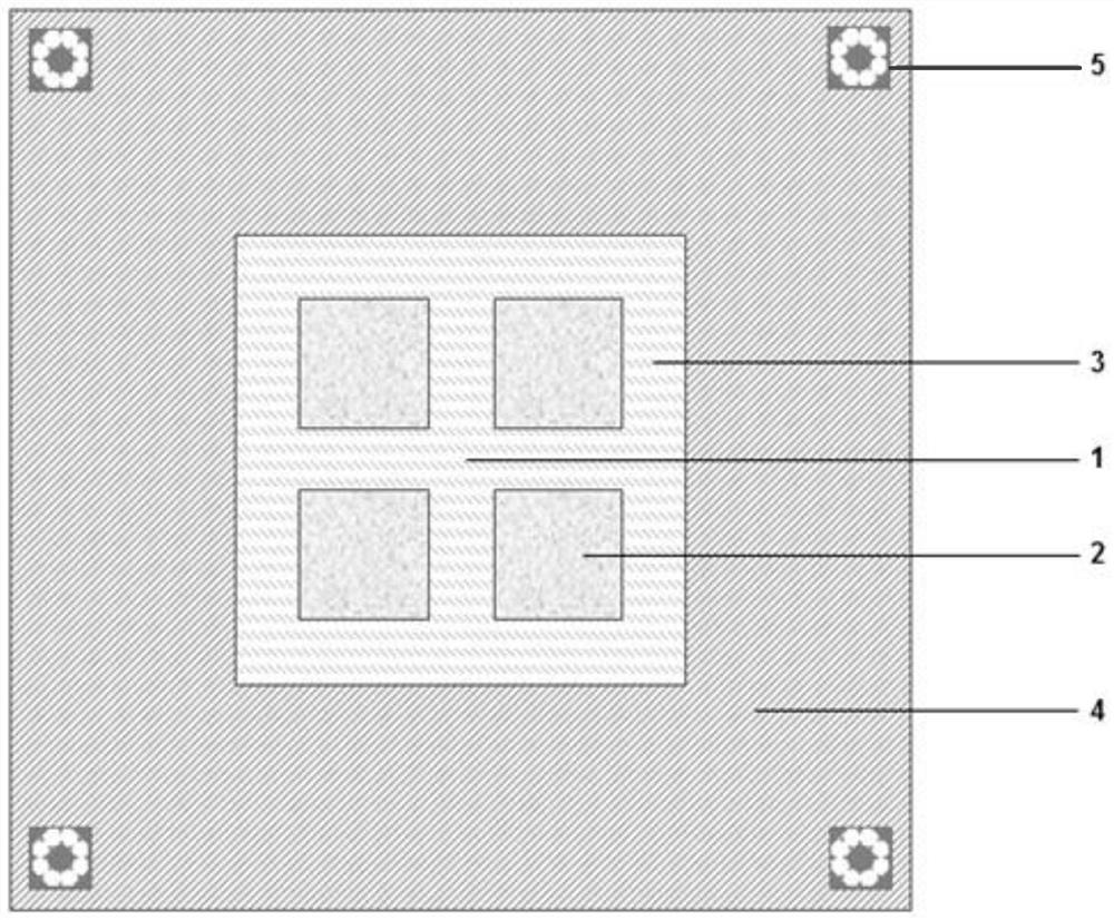
[0041] In order to solve the technical problems existing at present, the present invention provides an antistatic photomask, which mainly includes:
[0042] transparent substrate;
[0043] A photomask pattern arranged on the transparent substrate;
[0044] a conductive light-shielding layer, disposed on the transparent substrate at the periphery of the mask pattern, and spaced apart from the mask pattern;
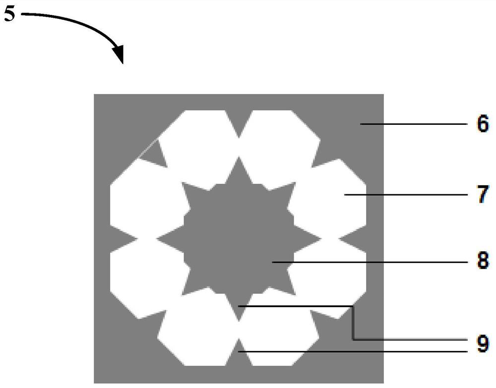
[0045] The discharge structure is arranged on the conductive light-shielding layer.
[0046] The antistatic photomask of the present invention is provided with a discharge structure on the conductive light-shielding layer on the periphery of the photomask pattern, which can guide a large amount of static charge accumulated on the large-area continuous conductive light-shielding layer outside the photomask pattern, and place it away from the photomask pattern area. Discharge is carried out, thereby avoiding the damaging effect of electrostatic charge directly discharging o...
PUM
| Property | Measurement | Unit |
|---|---|---|
| length | aaaaa | aaaaa |
| height | aaaaa | aaaaa |
| height | aaaaa | aaaaa |
Abstract
Description
Claims
Application Information

