SiOxNy-based synapse optically reading device and preparation method thereof

A neural synapse and optical reading technology, which is applied in optical components, biological neural network models, nanotechnology for materials and surface science, etc. Problems such as large interference, to achieve the effect of device size reduction and large bandwidth

Inactive Publication Date: 2018-06-01
UNIV OF ELECTRONIC SCI & TECH OF CHINA
View PDF8 Cites 13 Cited by
  • Summary
  • Abstract
  • Description
  • Claims
  • Application Information

AI Technical Summary

Problems solved by technology

Electrically read memristive bionic synapse with small transmission bandwidth and large mutual interference between signals

Method used


Image

  • SiOxNy-based synapse optically reading device and preparation method thereof

Examples


Embodiment 1

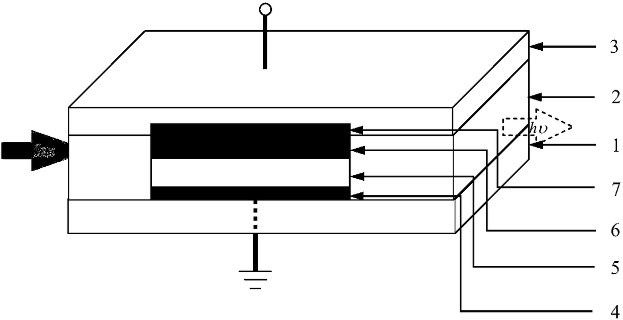
[0049] Such as figure 1 As shown, this embodiment provides a SiO-based x N y Optically readable synaptic devices, including surface plasmon waveguides and memristors;

[0050] The surface plasmon waveguide has "second metal layer 3 / SiN x Vertical three-layer structure of dielectric layer 2 / first metal layer 1";

[0051] The memristor has a vertical four-layer structure of "upper electrode 7 / second resistive layer 6 / first resistive layer 5 / lower electrode 4" arranged sequentially from top to bottom;

[0052] The memristor is embedded in the surface plasmon waveguide, the first resistive layer 5 and the second resistive layer 6 of the memristor serve as the optical signal propagation channel and the SiN of the surface plasmon waveguide x The medium layer 2 is connected horizontally.

[0053] The top of the upper electrode 7 is located inside the second metal layer 3 , which can reduce the loss of a part of the optical signal.

[0054] In this example,

[0055] The first r...

Embodiment 2

[0069] The difference between this embodiment and embodiment 1 is that

[0070] The thickness of the first metal layer 1 and the second metal layer 3 is 20nm;

[0071] The first resistive switch layer 5 is intrinsic SiO x N y Thin film, thickness is 50nm, adopts reactive magnetron sputtering method to obtain;

[0072] The second resistance variable layer 6 is SiO containing copper nanoparticles x N y The thin film, with a thickness of about 30nm and a copper content of 45% (volume percentage), is obtained by a co-sputtering method.

Embodiment 3

[0074] The difference between this embodiment and embodiment 1 is that

[0075] The thickness of the first metal layer 1 and the second metal layer 3 is 15nm;

[0076] The first resistive switch layer 5 is intrinsic SiO x N y Thin film, thickness is 40nm, adopts reactive magnetron sputtering method to obtain;

[0077] The second resistance variable layer 6 is SiO containing aluminum nanoparticles x N y A thin film with a thickness of about 40nm and an aluminum content of 40% (volume percentage) is obtained by a co-sputtering method.


PUM

PropertyMeasurementUnit
Thicknessaaaaaaaaaa
Thicknessaaaaaaaaaa
Thicknessaaaaaaaaaa

Abstract

The invention provides a SiOxNy-based synapse optically reading device and a preparation method thereof. The SiOxNy-based synapse optically reading device comprises a surface plasma waveguide and a memristor. The surface plasma waveguide has a vertical three-layer structure including a second metal layer, a SiNx dielectric layer, and a first metal layer which are successively arranged from top tobottom. The memristor has a vertical four-layer structure including an upper electrode, a second resistive layer, a first resistive layer, and a lower electrode which are successively arranged from top to bottom. The memristor is embedded in the surface plasma waveguide. The second resistive layer and the first resistive layer serve as optical signal propagation paths and are horizontally connected to the SiNx dielectric layer of the surface plasma waveguide. The SiOxNy-based synapse optically reading device optically read the weights of synapses such that a synapse optically reading device using the amplitude and phase of the optical signal as synaptic weights has advantages that cannot be equaled by a conventional neural synapse device using resistance as synaptic weights. The surface plasma waveguide can make the optical signal break through the diffraction limit for transmission, and is conducive to further reducing the size of the device.

Description

technical field [0001] The invention belongs to the technical field of silicon-based photonic integrated devices and neuromorphic chips, in particular to a SiO-based x N y Optically readable neurosynaptic devices and methods of making the same. Background technique [0002] For a memristor with a "metal / dielectric layer / metal" sandwich structure, if different bias voltages are applied, the resistance of the device will show a nonlinear change. This non-linear change in resistance is caused by the formation or disappearance of conductive channels in the dielectric layer under different bias voltages. However, the connection strength of this nanoscale filamentous conductive channel will vary with the magnitude and duration of the bias voltage. This property is very similar to the working mechanism of synapses connecting different neurons in the biological nervous system. It is this similarity between memristors and biological system synapses that makes them very suitable a...

Claims


Application Information

Patent Timeline
IPC IPC(8): H01L45/00B82Y30/00
CPCB82Y30/00H10N70/24H10N70/257H10N70/011H10N70/026B82Y20/00G02B2006/12035G02B6/1226G06N3/065G02B6/132H10N70/826H10N70/063H10N70/841H10N70/883
Inventor 李伟陈奕丞李东阳钟豪顾德恩蒋亚东
Owner UNIV OF ELECTRONIC SCI & TECH OF CHINA
Why Eureka
Try Eureka