SPR neurosynaptic device based on a-si memristive effect and its preparation method

A technology of neural synapse and memristor, which is applied in the field of bionic devices, can solve the problems of signal transmission crosstalk and small signal processing bandwidth, and achieve the effects of large signal processing bandwidth, strong anti-electromagnetic interference ability, and large bandwidth

Active Publication Date: 2020-07-31
UNIV OF ELECTRONICS SCI & TECH OF CHINA
View PDF9 Cites 0 Cited by
  • Summary
  • Abstract
  • Description
  • Claims
  • Application Information

AI Technical Summary

Problems solved by technology

[0004] In view of the above, the present invention provides an optical sensor based on the a-Si memristive effect for the problems of small signal processing bandwidth and prone to crosstalk in the signal transmission process existing in the existing memristor-based bionic synapse. Read SPR neural synaptic device and its preparation method

Method used


Image

  • SPR neurosynaptic device based on a-si memristive effect and its preparation method
  • SPR neurosynaptic device based on a-si memristive effect and its preparation method
  • SPR neurosynaptic device based on a-si memristive effect and its preparation method

Examples


Embodiment 1

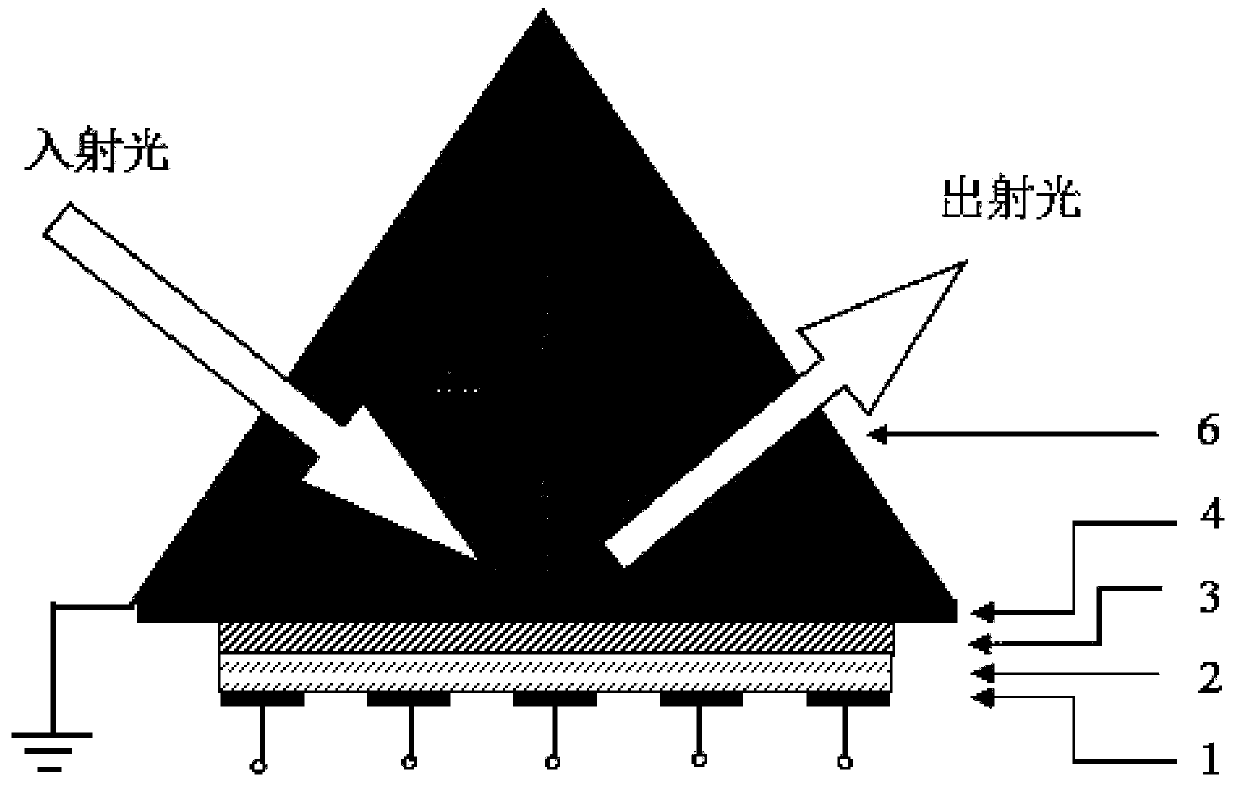
[0036] A SPR neurosynaptic device based on a-Si memristive effect, its structure is as figure 1 Shown: It includes a memristor and a crystalline silicon prism 6 arranged above the memristor. In this embodiment, the crystalline silicon prism 6 is a triangular prism processed from crystalline silicon, and the memristor has "Bottom electrode 1 / first a-Si resistive layer 2 / second a-Si resistive layer 3 / top electrode 4" vertical four-layer structure, in this embodiment, the top electrode 4 is deposited on the bottom surface of the crystalline silicon prism 6 Metallic silver Ag, the second a-Si resistive layer 3 is an a-Si film containing Ag nanoparticles, the volume fraction of Ag nanoparticles is 40%, and the first a-Si resistive layer 2 is an a-Si film containing Ag nanoparticles The a-Si film, the volume fraction of Ag nanoparticles is 5%, the top electrode 4 is metallic platinum Pt deposited on the bottom surface of the first a-Si resistive layer 2; the refractive index of ...

Embodiment 2

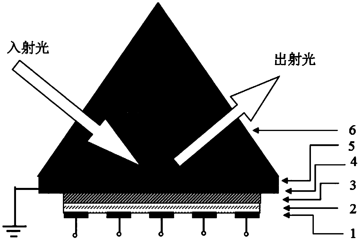
[0046] A SPR neurosynaptic device based on a-Si memristive effect, its structure is as figure 2 Shown: It includes a crystalline silicon wafer 5 and its supporting memristor and a crystalline silicon prism 6 arranged above the crystalline silicon wafer 5. In this embodiment, the crystalline silicon prism 6 is a triangular prism processed from crystalline silicon. The silicon wafer 5 is also made of crystalline silicon. The crystalline silicon wafer 5 and the crystalline silicon prisms 6 are preferably bonded with a refractive index matching liquid; the memristor has "bottom electrode 1 / first a" from bottom to top. -Si resistive layer 2 / second a-Si resistive layer 3 / top electrode 4" vertical four-layer structure. In this embodiment, the top electrode 4 is metallic silver Ag deposited on the bottom surface of the crystalline silicon wafer 5. The second a- The Si resistive layer 3 is an a-Si film containing Ag nanoparticles, and the volume fraction of Ag nanoparticles is 40%. The ...


PUM

PropertyMeasurementUnit
thicknessaaaaaaaaaa
thicknessaaaaaaaaaa
thicknessaaaaaaaaaa

Abstract

The invention relates to an SPR neurosynaptic device based on the a-Si memristive effect and a preparation method thereof, belonging to the technical field of bionic devices. The present invention couples the crystalline silicon prism with the memristor structure of "top electrode / a-Si: metal nanoparticle double resistive variable layer / bottom electrode", so that the optical signal under electrical modulation is injected into the double resistive variable layer through the crystalline silicon prism, And the surface plasmon resonance (SPR) effect is used to read the dielectric constant change information of the resistive layer during the working process of the device with optical signals, thereby realizing the optical reading of the synaptic weight of the device. The "electrical modulation, optical reading" neurosynaptic device proposed by the present invention has the incomparable advantages of the traditional "electrical modulation, electrical reading" synaptic device, because it not only has the traditional memristor's low energy consumption, non-volatile It also has the advantages of light as an information carrier for signal processing with large bandwidth and strong anti-electromagnetic interference ability.

Description

Technical field [0001] The invention belongs to the technical field of bionic devices, and specifically relates to a SPR neurosynaptic device based on a-Si memristive effect and a preparation method thereof. Background technique [0002] Traditional computers are based on the "von Neumann architecture". However, in the "von Neumann architecture", the data call and transmission between the information memory and the processor are connected through a bus, which makes information processing more efficient. It is not only affected by the processing speed and storage rate of the processor, but also restricted by the bus information transmission capacity, forming the so-called "von Neumann bottleneck." Although the human brain processes no less information than computers, it is obviously more efficient and consumes less energy. To this end, researchers have constructed the concept of intelligent computers, hoping to allow computers to learn neural networks to better simulate human bra...

Claims


Application Information

Patent Timeline
Patent Type & Authority Patents(China)
IPC IPC(8): H01L45/00
CPCH10N70/257H10N70/011
Inventor 李伟陈奕丞次会聚董湘刘诚李东阳蒋向东
Owner UNIV OF ELECTRONICS SCI & TECH OF CHINA
Why Eureka
Try Eureka