Method for testing recombination current of metal semiconductor interface

A technology of metal semiconductor and current density, which is applied in the direction of current density measurement, etc., can solve the problems of high cleaning cleanliness, inaccurate test results, and low accuracy

Active Publication Date: 2018-06-05
CSI SOLAR TECH (JIAXING) CO LTD
View PDF4 Cites 3 Cited by
  • Summary
  • Abstract
  • Description
  • Claims
  • Application Information

AI Technical Summary

Problems solved by technology

[0004] Since no metal can appear during the QSSPC test, the existing test method needs to corrode the sintered metal in the sample to be tested first, and the corrosion process will destroy the surface state of the non-metallic area
The corroded metal needs to be completely cleaned, and QSSPC has high requirements on the cleanliness of the cleaning, otherwise the test results will be inaccurate or the test data will not be available.
Moreover, since the metal will be corroded during the QSSPC test, the measured metal interface recombination current density is the interface recombination current density after corroding the metal, that is, the measured result is an equivalent value, not the real recombination current density of the metal interface
[0005] The composite current density test method of the metal interface in the prior art is complicated to operate, requires high cleaning and cleanliness, and the test results fluctuate greatly and the accuracy is not high

Method used


Image

  • Method for testing recombination current of metal semiconductor interface
  • Method for testing recombination current of metal semiconductor interface
  • Method for testing recombination current of metal semiconductor interface

Examples


Embodiment Construction

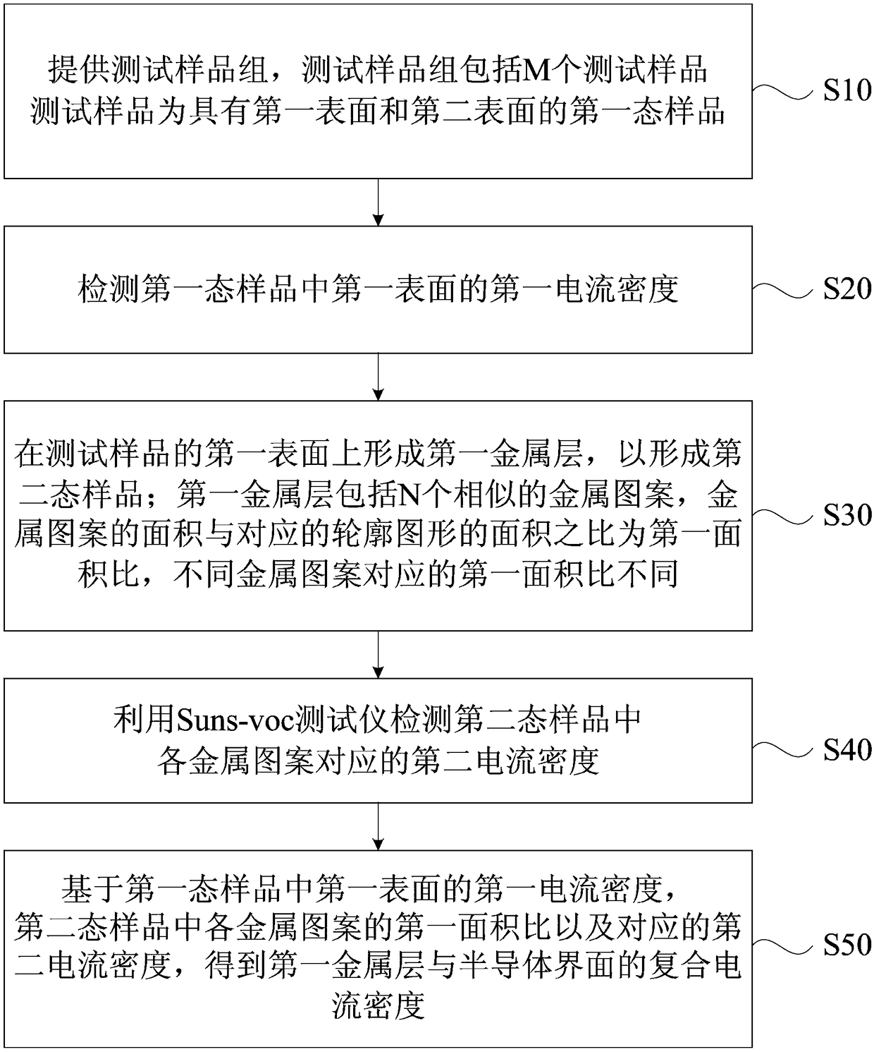
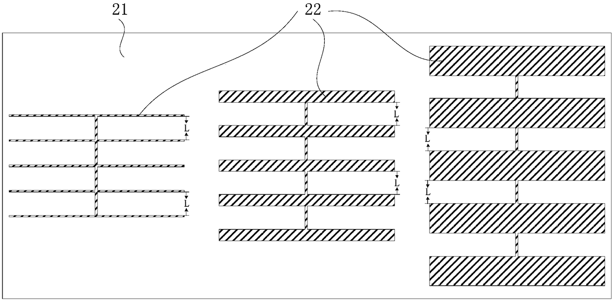
[0032] The present invention will be further described in detail below in conjunction with the accompanying drawings and embodiments. It should be understood that the specific embodiments described here are only used to explain the present invention, but not to limit the present invention. In addition, it should be noted that, for the convenience of description, only some structures related to the present invention are shown in the drawings but not all structures.

[0033] figure 1 It is a flowchart of a test method for recombination current density at a metal-semiconductor interface provided by an embodiment of the present invention. see figure 1 , an embodiment of the present invention provides a method for testing the recombination current density at a metal-semiconductor interface, including:

[0034] S10. Provide a test sample group, the test sample group includes M test samples, the test sample is a first-state sample having a first surface and a second surface, where...


PUM


Abstract

The invention discloses a method for testing the recombination current of a metal semiconductor interface. The method for testing the recombination current of the metal semiconductor interface comprises the following steps: providing a test sample set, wherein test samples are first samples provided with first surfaces and second surfaces; detecting the first current density of the first surfacesin the first samples; forming first metal layers on the first surfaces so as to form second samples, wherein each first metal layer comprises N similar metal patterns, and first area ratios corresponding to different metal patterns are different; using a Suns-Voc tester to detect second current density corresponding to each metal pattern in the second samples; and based on the first current density, the first area ratio of each metal pattern and the corresponding second current density, obtaining the recombination current density of the first metal layer and the semiconductor interface. According to the scheme provided by the invention, the recombination current density testing for the metal semiconductor interface is realized simply and quickly, and the effect that the test result is trueand accurate is achieved.

Description

technical field [0001] The embodiment of the present invention relates to a current density testing technology, in particular to a testing method for the recombination current density of a metal-semiconductor interface. Background technique [0002] The recombination current density between metal and semiconductor interfaces has important applications in many fields. For example, the recombination of carriers in a solar cell is one of the most important factors affecting the efficiency of a solar cell, and the recombination at the metal-semiconductor interface occupies an important proportion. Accurate and convenient testing of the recombination current density at the metal-semiconductor interface plays an important role in improving battery design and optimizing process technology. [0003] At this stage, the metal paste separating the parallel line patterns is printed on the semiconductor material and sintered to form the sample to be tested. When measuring the recombina...

Claims


Application Information

Patent Timeline
Patent Type & Authority Applications(China)
IPC IPC(8): G01R19/08
CPCG01R19/08
Inventor 万松博邓伟伟蒋方丹邢国强
Owner CSI SOLAR TECH (JIAXING) CO LTD
Why Eureka
Try Eureka