Aging treatment method and aging treatment system applied to display panel

A technology of aging treatment and display panel, which is applied in the direction of static indicators, instruments, semiconductor/solid-state device testing/measurement, etc. It can solve problems such as inability to produce good aging effects, increase the cut-off voltage range, ensure process yield, good effect

Active Publication Date: 2020-05-05
BOE TECH GRP CO LTD +1
View PDF7 Cites 0 Cited by
  • Summary
  • Abstract
  • Description
  • Claims
  • Application Information

AI Technical Summary

Problems solved by technology

[0004] Embodiments of the present invention provide an aging treatment method and aging treatment system applied to display panels to solve the problem in the prior art that a single fixed Aging Stress cannot make all products achieve good aging effects

Method used


Image

  • Aging treatment method and aging treatment system applied to display panel
  • Aging treatment method and aging treatment system applied to display panel
  • Aging treatment method and aging treatment system applied to display panel

Examples


Embodiment Construction

[0059] In order to make the objectives, technical solutions and advantages of the present invention clearer, the present invention will be further described in detail below in conjunction with the accompanying drawings. Obviously, the described embodiments are only a part of the embodiments of the present invention, rather than all of them. Based on the embodiments of the present invention, all other embodiments obtained by those of ordinary skill in the art without creative work shall fall within the protection scope of the present invention.

[0060] The shapes and sizes of the components in the drawings do not reflect the true proportions, and are only intended to illustrate the content of the present invention schematically.

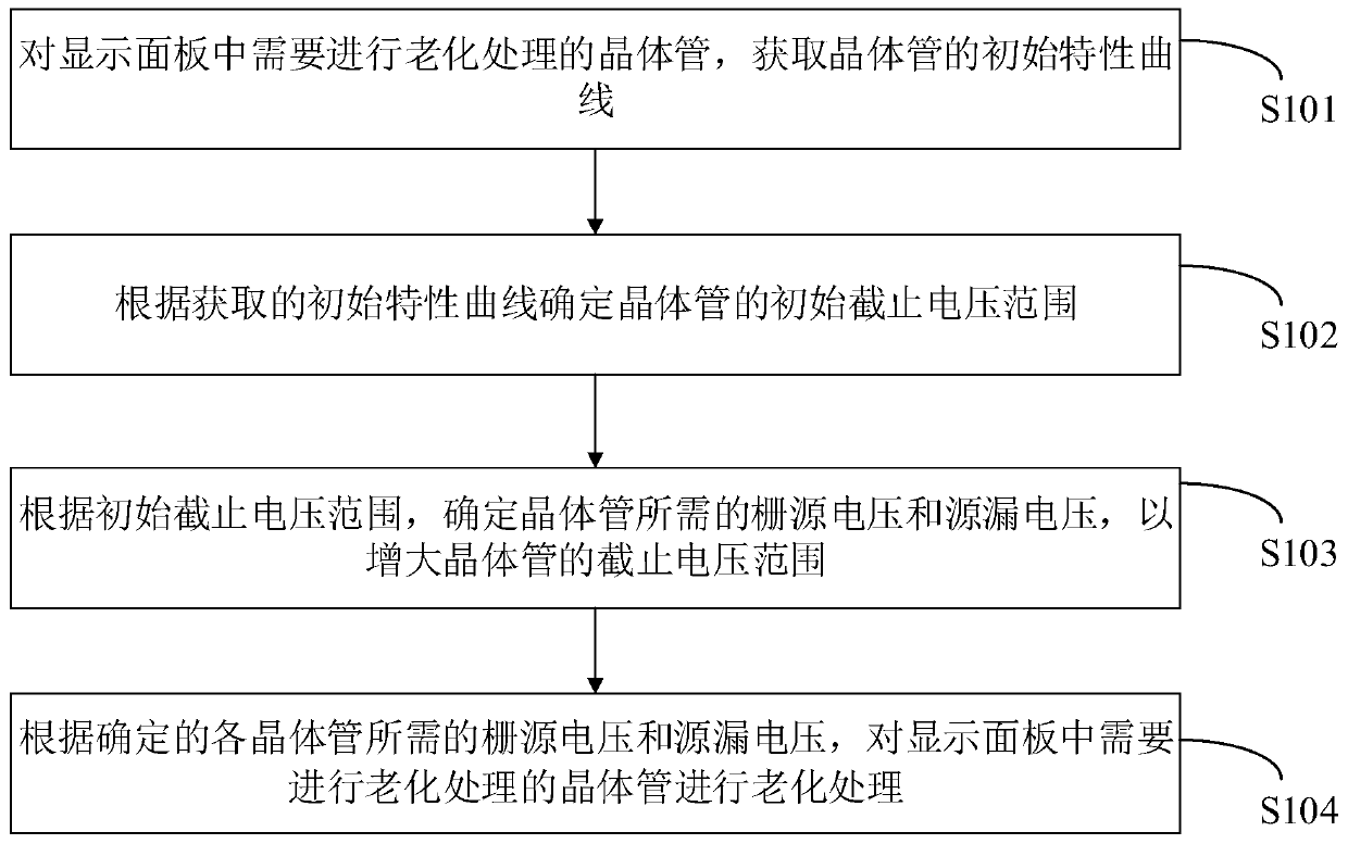
[0061] An embodiment of the present invention provides an aging treatment method for transistors applied to a display panel, such as figure 1 Shown, including:

[0062] S101. Obtain an initial characteristic curve of the transistor in the display panel that...


PUM


Abstract

The invention discloses an aging treatment method and an aging treatment system applied to a display panel. The initial cut-off voltage range of the transistor is determined according to the initial characteristic curve of the transistor that needs aging treatment in the display panel; and the initial cut-off voltage range is determined according to the initial cut-off voltage range. The gate-source voltage and drain-source voltage required by the transistor to increase the cut-off voltage range of the transistor; according to the determined gate-source voltage and drain-source voltage required by each transistor, perform aging treatment on the transistors that need aging treatment in the display panel . In this method, since the aging treatment voltage applied to each display panel is obtained according to the transistors in the display panel, the effect after aging treatment is good, and the process yield and the stability of product TFT characteristics can be effectively guaranteed.

Description

Technical field [0001] The invention relates to the field of display technology, in particular to an aging treatment method and aging treatment system applied to a display panel. Background technique [0002] In the manufacturing process of Organic Light Emitting Diode (OLED) devices, the Thin Film Transistor (TFT) in the OLED device needs to be aged (Aging), referred to as TFT-Aging, to achieve The purpose of eliminating bright spots and ensuring stable TFT characteristics. At present, during the TFT-Aging process, by applying a fixed voltage value to the OLED device, a relatively large stress is formed to act on the TFT, thereby achieving an aging effect. The aging effect is related to Stress, and moderate Stress can increase the yield of OLED devices and increase the stability of TFT characteristics. [0003] At this stage, TFT-Aging is to write a fixed voltage value to the TFT to form a fixed Stress (Vgs and Vds) to act on the TFT, and through multiple debugging, the ideal Ag...

Claims


Application Information

Patent Timeline
Patent Type & Authority Patents(China)
IPC IPC(8): G01R31/27H01L27/32
CPCG01R31/275H10K59/12H01L27/1296G09G3/3233G09G2310/0251G09G2310/0262G09G2300/0819G09G2300/0842H01L22/20H10K71/00H10K59/1201H10K71/831
Inventor 赵科张国庆高弘玮王晓伟贾智慧宗岩杨龙飞杨红霞郭美利王伟峰赵普查郭志鑫
Owner BOE TECH GRP CO LTD
Why Eureka
Try Eureka