
GaN material-based LED chip and LED lamp

A LED chip and chip technology, applied in the direction of electrical components, circuits, semiconductor devices, etc., can solve the problems of light reduction, difficult packaging, poor reliability, etc., and achieve the effects of LED cost reduction, integration improvement, and flexible color temperature adjustment

Inactive Publication Date: 2018-06-08
XIAN ZHISHENG RUIXIN SEMICON TECH CO LTD
View PDF0 Cites 0 Cited by
  • Summary
  • Abstract
  • Description
  • Claims
  • Application Information

AI Technical Summary

Problems solved by technology

In the prior art, a single light-emitting chip can only emit monochromatic light. If light of other colors needs to be synthesized, light-emitting chips of different colors need to be mixed together and filled with a large amount of phosphor powder. difficult problem
In addition, when light is incident into the phosphor layer, there will be strong scattering, which will cause the phosphor layer to absorb light, causing a large amount of light to be reflected, that is, the light transmitted through the phosphor layer will be significantly reduced.

Method used


Image

  • GaN material-based LED chip and LED lamp
  • GaN material-based LED chip and LED lamp
  • GaN material-based LED chip and LED lamp

Examples


Embodiment 1

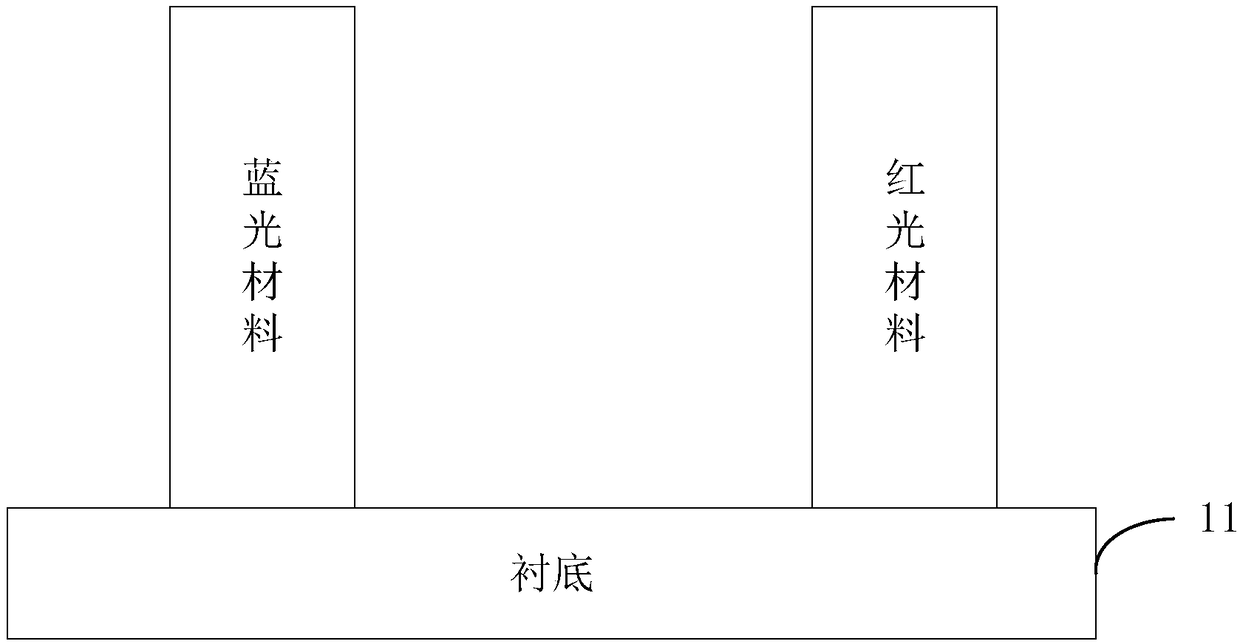
[0029] Such as figure 1 As shown, figure 1 A schematic diagram of the structure of a GaN-based LED chip provided by the present invention, the chip includes:

[0030] Substrate (11);

[0031] At least one blue light material and at least one red light material are grown on the substrate (11).

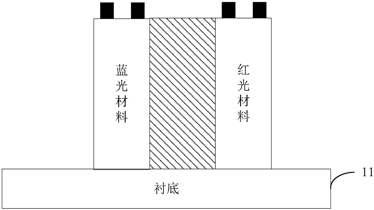
[0032] Further, on the basis of the above-mentioned embodiments, the chip further includes an isolation wall, which is arranged between the blue light material and the red light material, and is used to isolate the blue light material and the red light material.

[0033] Further, on the basis of the foregoing embodiment, the chip further includes electrodes, which are arranged on the blue light material and the red light material. Specifically, see figure 2 , figure 2 It is a schematic diagram of another GaN-based LED chip structure provided by the present invention.

[0034] Further, on the basis of the foregoing embodiments, the blue light material includes a first GaN buffer layer (101), a ...

Embodiment 2

[0042] The present invention also provides a method for preparing an LED light source based on a blue light material and a red light material. The LED chip of the first embodiment is prepared by the method of this embodiment, and the method includes:

[0043] Choose sapphire as the substrate (11);

[0044] Growing a blue light material on the substrate (11), the blue light material being used to generate blue light driven by a blue driving voltage;

[0045] Selectively etching the blue light material to form a red light wick groove;

[0046] Growing a red light material in the red light wick groove, the red light material being used to generate red light under the driving of a red light driving voltage;

[0047] Electrodes are prepared on the blue light material and the red light material respectively to complete the preparation of the LED light source based on the blue light material and the red light material.

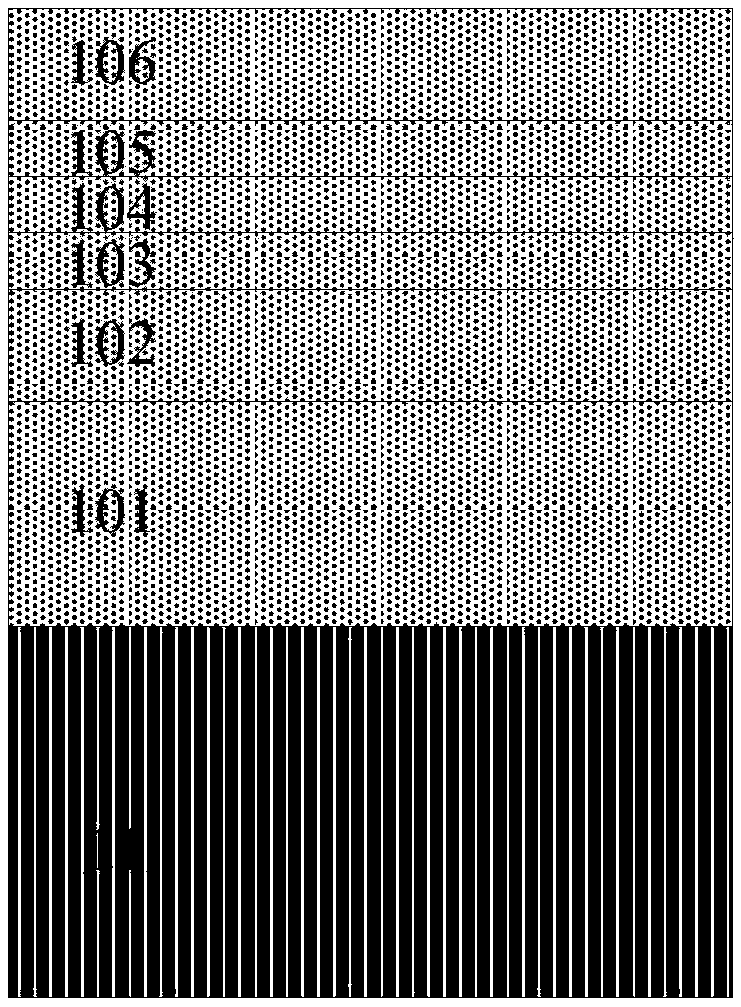
[0048] See image 3 , image 3 This is a schematic diagram of a blue light...


PUM


Abstract

The invention provides a GaN material-based LED chip, which comprises a substrate (11), at least one blue light material and at least one red light material, wherein the at least one blue light material and the at least one red light material grow on the substrate (1). The GaN material-based LED chip has the beneficial effects that (1) light of multiple colors can be generated on one chip and thedosage of fluorescent powder is relatively small; (2) the integration level is improved and the cost of an LED can be reduced; and (3) color temperature adjustment is more flexible.

Description

Technical field [0001] The present invention relates to the field of semiconductor technology, in particular to an LED chip and an LED lamp based on GaN material. Background technique [0002] LED light sources are more and more commonly used in the lighting field. Generally, the LED light source emits various colors of light through the LED light-emitting chip and phosphor powder. In the prior art, a single light-emitting chip can only emit monochromatic light. If it is necessary to synthesize light of other colors, it is necessary to mix light-emitting chips of different colors and fill them with a large amount of phosphor. This results in poor reliability and packaging. Difficult question. In addition, the light incident on the phosphor adhesive layer will cause a strong scattering phenomenon, which makes the phosphor adhesive layer absorb light, causing a large amount of light to be reflected, that is, the light transmitted through the phosphor layer will be significantly r...

Claims


Application Information

Patent Timeline
Patent Type & Authority Applications(China)
IPC IPC(8): H01L33/32H01L33/06H01L33/44H01L33/00
CPCH01L33/32H01L33/0075H01L33/06H01L33/44
Inventor 左瑜
Owner XIAN ZHISHENG RUIXIN SEMICON TECH CO LTD
Learn More