
Steel mesh for printing printed circuit boards and printing machine

A technology for printed circuit boards and printing machines, applied to screen printing machines, printing machines, rotary printing machines, etc., can solve problems such as high cost, unfavorable large-scale production, and inability to place printed circuit boards 6, and reduce The effect of saving production cost and printing machine cost

Pending Publication Date: 2018-06-15
FENGHUO COMM SCI & TECH CO LTD
View PDF8 Cites 0 Cited by
  • Summary
  • Abstract
  • Description
  • Claims
  • Application Information

AI Technical Summary

Problems solved by technology

[0007] But in fact, the shape of printed circuit boards of electronic products is rich and varied, especially for large-scale equipment, such as communication equipment and servers, etc., the size of printed circuit boards is often very large, and the long side exceeds 650mm or even 1m, such as Image 6 and Figure 7 As shown, for this type of large-size printed circuit board 6, if a conventional printing machine and stencil are used, the printed circuit board 6 will not be able to be placed between the two stencil brackets 5 of the stencil
like Figure 4 As shown, that is, the printed circuit board 6 can only be placed under the two stencil brackets 5, and cannot be closely attached to the stencil 2, and the first step of the SMT solder paste printing process cannot be realized.
However, if a corresponding printing machine is set up for each size, the cost is high and it is not conducive to mass production

Method used


Image

  • Steel mesh for printing printed circuit boards and printing machine
  • Steel mesh for printing printed circuit boards and printing machine
  • Steel mesh for printing printed circuit boards and printing machine

Examples


no. 1 example

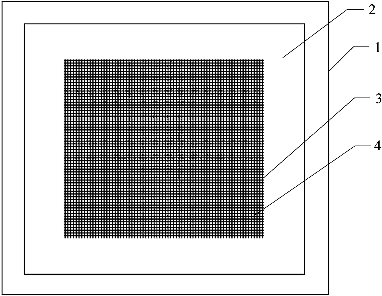
[0038] Such as Figure 7 As shown, the present invention is used for the stencil of printed circuit board, comprises screen frame 1 and omentum 2, and omentum 2 is positioned at the bottom surface of screen frame 1, and the middle part of omentum 2 is provided with opening area 3, and opening area 3 is provided with a plurality of mesh holes 4 for solder paste deposition, and the mesh frame is a rectangular frame, preferably a square frame. A group of opposite frames of the screen frame 1 are respectively provided with slots 11 (shown by dotted lines in the figure), and the two slots 11 are matched with the two steel screen brackets 5 of the printing machine respectively. When the screen frame 1 is supported between two stencil brackets 5 , the plane where the omentum 2 is located is not higher than the bottom surface of the two stencil brackets 5 . Because the omentum 2 is lower than the bottom surfaces of the two steel mesh brackets 5, or the bottom surfaces of the omentum ...

no. 2 example

[0040] Such as Figure 7 , Figure 8 and Figure 9 As shown, the stencil bracket 5 of the printing machine includes a limiting plate 51 and a supporting plate 52, the limiting plate 51 is arranged on the outside of the outer wall of the screen frame 1, and the limiting plates 51 of the two stencil brackets 5 are used to The stencil is confined within it. The supporting plate 52 is arranged vertically to the limiting plate 51, and is used to support the screen frame 1 of the steel mesh. Specifically, the steel mesh bracket 5 has an L-shaped cross section, its long side is a limiting plate 51 , and its short side is a supporting plate 52 . In this embodiment, the slot 11 is located on the bottom of a group of opposite frames, and the slot 11 forms a step on the bottom of the frame, so that the interface of the stencil in the direction where the printed circuit board 6 enters has an inverted convex shape. The supporting plate 52 is located in the slot 11, that is, in the gap of...

no. 3 example

[0042] Such as Figure 7 , Figure 8 and Figure 9 As shown, the stencil bracket 5 of the printing machine includes a limiting plate 51 and a supporting plate 52, the limiting plate 51 is arranged on the outside of the outer wall of the screen frame 1, and the limiting plates 51 of the two stencil brackets 5 are used to The stencil is confined within it. The supporting plate 52 is arranged vertically to the limiting plate 51, and is used to support the screen frame 1 of the steel mesh. Specifically, the steel mesh bracket 5 has an L-shaped cross section, its long side is a limiting plate 51 , and its short side is a supporting plate 52 . In this embodiment, the slot 11 is located on the bottom of a group of opposite frames, and the slot 11 forms a step on the bottom of the frame, so that the interface of the stencil in the direction where the printed circuit board 6 enters has an inverted convex shape. The supporting plate 52 is located in the slot 11 , that is, in the not...


PUM


Abstract

The invention discloses a steel mesh for printing printed circuit boards and a printing machine, and relates to the technical field of surface mounting. A stencil comprises a mesh frame and a mesh film, the mesh film is provided with a plurality of mesh holes for solder paste deposition, a set of opposite frames of the mesh frame is provided with slottings matched with two stencil brackets of theprinting machine, when the mesh frame is supported between the two stencil brackets, the plane of the mesh film is not higher than the bottom of the stencil brackets, the mesh film of the stencil sinks to the bottom of two stencil brackets to accommodate a larger printed circuit board to ensure that the printed circuit board is attached to the mesh film, so that the production cost is reduced, andthe stencil is suitable for mass production.

Description

technical field [0001] The invention relates to the field of surface mount technology (Surface Mount Technology, SMT), in particular to a stencil for printing printed circuit boards and a printing machine. Background technique [0002] With the continuous improvement of the function and performance of system equipment, the density of components on the Printed Circuit Board (PCB), an important hardware component in the system, is getting higher and higher. Surface mount devices on the printed circuit board It is getting denser and more numerous, and it is no longer possible to manufacture it by hand. At present, for such printed circuit boards with larger surface mount devices, SMT technology is generally used, and the entire SMT process is completed by a machine through a series of processes. Among them, the first link of the SMT process is the solder paste printing link. In the solder paste printing link, it is necessary to use a solder paste printing machine and a stencil...

Claims


Application Information

Patent Timeline
Patent Type & Authority Applications(China)
IPC IPC(8): B41F15/36B41F15/26
CPCB41F15/26B41F15/36B41P2217/50
Inventor 刘志炉
Owner FENGHUO COMM SCI & TECH CO LTD
Learn More