
An electronic component and its manufacturing method

A technology of electronic components and manufacturing methods, which is applied in the direction of electrical components, inductance/transformer/magnet manufacturing, circuits, etc., can solve the problems of high cost, substrate flatness, high compactness, and difficult to realize electrode production, etc., to achieve Reduce costs, improve production effects, and use a wide range of effects

Active Publication Date: 2021-02-02
SHENZHEN SUNLORD ELECTRONICS
View PDF8 Cites 0 Cited by
  • Summary
  • Abstract
  • Description
  • Claims
  • Application Information

AI Technical Summary

Problems solved by technology

The traditional yellow light process has high requirements on the flatness and compactness of the substrate, and it is difficult to realize the electrode production with a wire diameter and line spacing of less than 15 μm. Although the thin film process can realize the production of fine electrodes, it has special requirements for ceramic materials. required and costly

Method used


Image

  • An electronic component and its manufacturing method

Examples


example 1

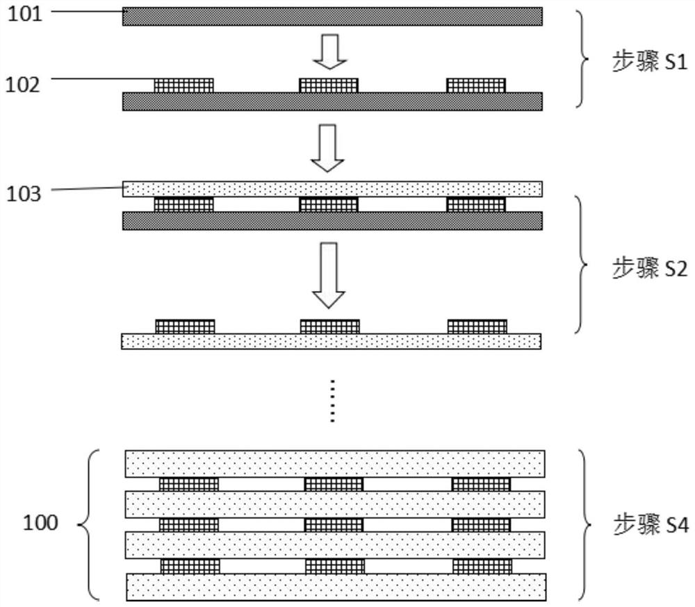
[0042] Using the manufacturing method of the above-mentioned electronic components to manufacture metric 0806 laminated chip common mode inductors includes the following steps: using organic thin film transfer electrodes, transferring the fine electrodes to the inorganic thin film substrates, laminating them to form ceramic green bodies, and then Cutting, debinding, sintering, chamfering, making terminal electrodes and electroplating are sequentially completed on the ceramic green body to complete the production of electronic components. specifically:

[0043] 1) making conductive electrodes on the organic film substrate;

[0044] 1.1) Prepare the organic film substrate

[0045] Purchase PANAC's TP-01 release transfer film.

[0046] 1.2) Making conductive electrodes

[0047] 1.2.1) Equipped with conductive paste: the silver paste of L6112 produced by Dupont Company, with a volume resistivity of 0.022mm*ohm;

[0048] 1.2.2) Use screen printing equipment to coat the conducti...

example 2

[0063] The metric 0806 multilayer chip common mode inductor is produced by the above-mentioned manufacturing method of electronic components. The difference between the steps and the example 1 is that step 2.3) is: use 300-800mJ / cm for the bonded substrate 2 The UV light is used for illumination; step 2.4) is: after the above UV illumination is completed, the organic film is torn off, and at this time the electrode has been transferred to the inorganic film substrate. Among them, the metric 0806 multilayer chip common mode inductor, the line width and line spacing can also be reduced by 50% compared with the traditional yellow light process. A drop of 30% to 35%.

example 3

[0065] Manufacturing metric 0605 multilayer chip common mode inductors by using the manufacturing method of the above-mentioned electronic components includes the following steps: transferring the fine electrodes to the inorganic thin film substrate by means of organic thin film transfer electrodes, performing lamination to form a ceramic green body, and then Cutting, debinding, sintering, chamfering, making terminal electrodes and electroplating are sequentially completed on the ceramic green body to complete the production of electronic components. specifically:

[0066] 1) making conductive electrodes on the organic film substrate;

[0067] 1.1) Prepare the organic film substrate

[0068] Purchase PANAC's TP-01 release transfer film.

[0069] 1.2) Making conductive electrodes

[0070] 1.2.1) Equipped with conductive paste: L6112 silver paste produced by Dupont Company, with a volume resistivity of 0.022mm*ohm;

[0071] 1.2.2) The conductive electrode paste is coated on ...


PUM

PropertyMeasurementUnit
thicknessaaaaaaaaaa
widthaaaaaaaaaa

Abstract

The invention discloses an electronic component and a manufacturing method thereof, wherein the manufacturing method includes: S1: making electrodes on an organic film; S2: transferring the electrodes on the organic film to an inorganic film substrate; S3: repeating Steps S1 and S2, forming a plurality of inorganic thin film substrates loaded with electrodes; S4: making a plurality of inorganic thin film substrates loaded with electrodes into a green body through a lamination process, and then performing sintering. The invention realizes the production requirements of the fine electrode, and its cost is greatly reduced compared with the thin film technology, and its application range is wider than that of the thin film technology.

Description

technical field [0001] The invention relates to an electronic component and a manufacturing method thereof. Background technique [0002] With the rapid development of smart phones, it is required to further miniaturize, thin, and low-cost laminated chip devices. While the appearance size is miniaturized, the performance of the device must be guaranteed, which requires the internal electrode structure to be more refined and complete. The traditional yellow light process has high requirements on the flatness and compactness of the substrate, and it is difficult to realize the electrode production with a wire diameter and line spacing of less than 15 μm. Although the thin film process can realize the production of fine electrodes, it has special requirements for ceramic materials. requirements and high cost. [0003] The disclosure of the above background technical content is only used to assist in understanding the concept and technical solution of the present invention, and...

Claims


Application Information

Patent Timeline
Patent Type & Authority Patents(China)
IPC IPC(8): H01F41/00
CPCC04B35/10C04B2235/3274C04B2235/3279C04B2235/365C04B2235/442
Inventor 郑卫卫陈柳城
Owner SHENZHEN SUNLORD ELECTRONICS
Learn More