Sputtering target-backing plate assembly
A technology of backing plate and sputtering target, which is applied in sputtering coating, welding equipment, ion implantation coating, etc., to achieve the effect of suppressing the generation of powder particles, reducing the failure rate, and uniform film formation
- Summary
- Abstract
- Description
- Claims
- Application Information
AI Technical Summary
Problems solved by technology
Method used
Image

Examples
Embodiment 1
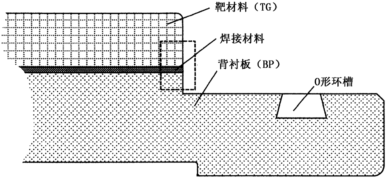
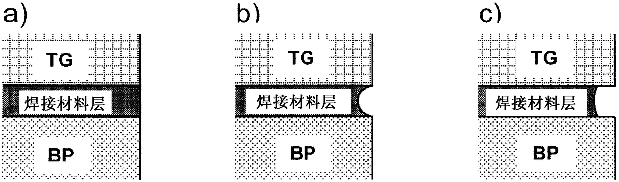
[0085] A disk-shaped single-crystal silicon (Si) target with a diameter of 330 mm and a disk-shaped oxygen-free copper (OFC) backing plate were joined so that the average layer thickness of indium (In) as a solder material was 0.28 mmt ( bonding).
[0086] Next, the indium solder material existing between the target and the backing plate was shaved off by 0.28 mm on one side from the side surface of the target, and dimples were formed on the entire outer periphery.
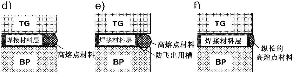
[0087] Next, a copper wire having a diameter of 0.3 mm and a purity of 4N was fitted into the recess with a resin spatula, thereby obtaining a sputtering target-backing plate assembly. Next, this assembly was installed in a sputtering apparatus, sputtering was performed, and the generation amount of powder particles was detected.
[0088] In the evaluation of powder particles, a film is formed on a dummy wafer with a power of 2000W. At the same time, every time 1 kWh is passed, a monitor wafer is placed. At this ...
Embodiment 2
[0097] A disk-shaped single crystal silicon (Si) target with a diameter of 330 mm and a disk-shaped molybdenum backing plate were bonded so that the average layer thickness of indium (In) as a solder material was 0.45 mmt.
[0098] On the upper surface of the backing plate, a groove with a width of 0.2 mm and a depth of 0.1 mm is processed in advance based on the point 0.3 mm inward from the periphery.
[0099] Next, the indium solder material existing between the target and the backing plate was shaved off by 0.5 mm one side from the side surface of the target, including scooping out the indium that had entered the above-mentioned groove, while forming pits on the entire periphery.
[0100] Next, a molybdenum wire with a diameter of 0.6 mm and a purity of 3N5 whose surface was roughened to Ra 5 μm with sandpaper was inserted into the cavity with a resin spatula to obtain a sputtering target-backing plate assembly. Next, this assembly was installed in a sputtering apparatus, s...
Embodiment 3-11、 comparative example 3-11
[0108] In addition, with the combinations described in Table 1, the number of particles on the substrates formed in the same manner by the sputtering test was compared.
PUM
| Property | Measurement | Unit |
|---|---|---|
| melting point | aaaaa | aaaaa |
| surface roughness | aaaaa | aaaaa |
| surface roughness | aaaaa | aaaaa |
Abstract
Description
Claims
Application Information
 - R&D
- Intellectual Property
- Life Sciences
- Materials
- Tech Scout
- Unparalleled Data Quality
- Higher Quality Content
- 60% Fewer Hallucinations
Browse by: Latest US Patents, China's latest patents, Technical Efficacy Thesaurus, Application Domain, Technology Topic, Popular Technical Reports.
© 2025 PatSnap. All rights reserved.Legal|Privacy policy|Modern Slavery Act Transparency Statement|Sitemap|About US| Contact US: help@patsnap.com