Manufacturing method for color filter substrate and color filter substrate

A color filter and production method technology, applied in optics, nonlinear optics, instruments, etc., can solve the problems of horn or horn step difference, affecting the process, affecting product quality, etc., to avoid horn or horn step difference, and ensure product quality. Effect

Inactive Publication Date: 2018-06-29
TCL CHINA STAR OPTOELECTRONICS TECH CO LTD
View PDF4 Cites 4 Cited by
  • Summary
  • Abstract
  • Description
  • Claims
  • Application Information

AI Technical Summary

Problems solved by technology

Among them, such as figure 1 As shown, the color filter substrate generally includes a substrate 10, a black matrix 20 (Black Matrix, BM) formed on the substrate 10, a color filter layer 30, and a transparent electrode layer 40 formed on the color filter layer 30 And the spacer 50 formed on the transparent electrode layer 40; wherein, the color filter layer 30 includes a plurality of filter units 31 of different colors, for example, red, green and blue photosensitive resins are used to form red, green and blue respectively. The blue filter unit, the black matrix 20 is used to define the boundary between each filter unit 31, in order to prevent light leakage between adjacent filter units 31, the edge of the filter unit 31 is usually overlapped with the black matrix 20, At this time, due to the existence of the lower black matrix 20, when the edges of each filter unit 31 are overlapped by the black matrix 20, it is easy to form horns or corner differences, which will affect the subsequent process, such as causing the transparent electrode layer 40 of the subsequent process to break. , affecting product quality

Method used


Image

  • Manufacturing method for color filter substrate and color filter substrate
  • Manufacturing method for color filter substrate and color filter substrate
  • Manufacturing method for color filter substrate and color filter substrate

Examples


Embodiment Construction

[0032] In order to further illustrate the technical means adopted by the present invention and its effects, the following describes in detail in conjunction with preferred embodiments of the present invention and accompanying drawings.

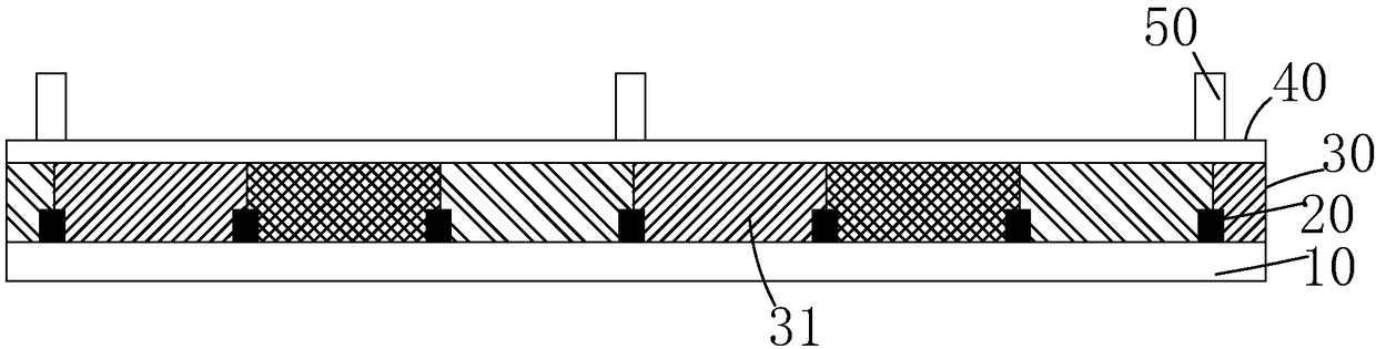
[0033] see Figure 7 , the invention provides a method for manufacturing a color filter substrate, comprising the following steps:

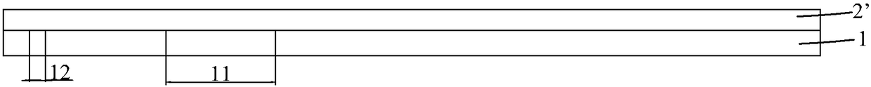
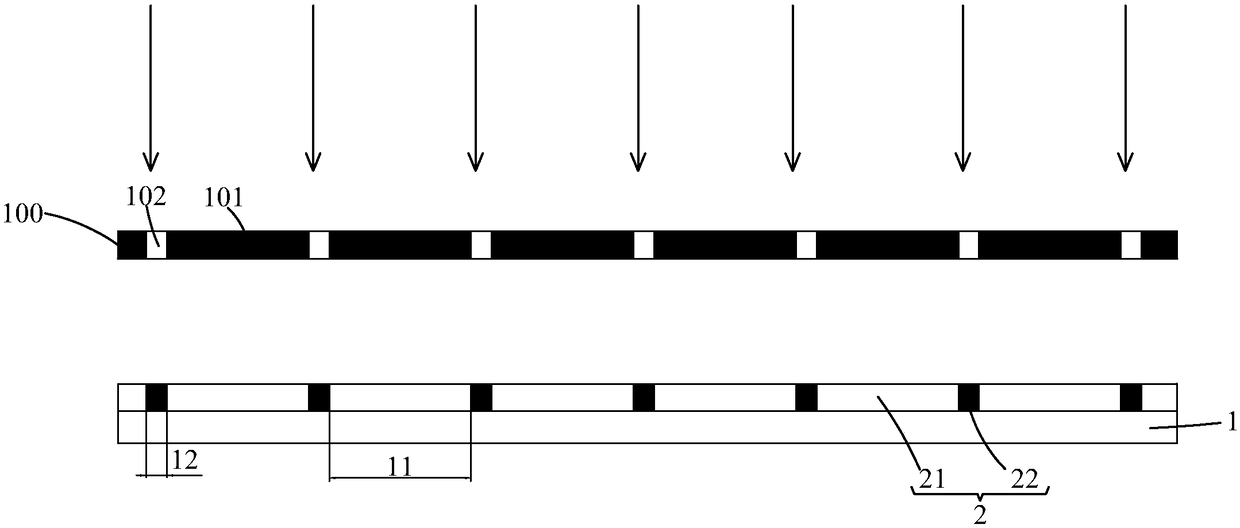
[0034] Step S1, such as figure 2 As shown, a substrate 1 is provided, and the substrate 1 includes a plurality of pixel regions 11 arranged in an array and non-pixel regions 12 located between adjacent pixel regions 11 .

[0035] Wherein, the pixel area 11 is used to form the sub-pixels of the liquid crystal display panel, so as to form a display screen by emitting light of different colors from the sub-pixels, and each non-pixel area 12 is used to form a light shielding member separating each sub-image (such as black matrix) to prevent color mixing between different subpixels.

[0036] Step S2, such as fig...


PUM


Abstract

The invention provides a manufacturing method for a color filter substrate and the color filter substrate. The manufacturing method for the color filter substrate comprises the following steps that the substrate is provided, wherein the substrate comprises multiple pixel areas which are distributed in an array and non-pixel areas located among the adjacent pixel areas; transparent light resistancethin film is formed on the substrate; the light resistance thin film in the non-pixel areas is subjected to carbonization treatment to obtain a light resistance layer, wherein the light resistance layer comprises transparent parts in all the pixel areas and light shielding parts in all the non-pixel areas; a color filter layer is formed on the light resistance layer. Light shielding is conductedthrough the light shielding parts in the light resistance layer, the function of a black matrix is achieved, the color filter layer is subjected to bottom flatting through the transparent parts in thelight resistance layer, cattle horns or corner segment differences on the color filter layer are avoided, and the product quality is guaranteed.

Description

technical field [0001] The invention relates to the field of display technology, in particular to a method for manufacturing a color filter substrate and the color filter substrate. Background technique [0002] A Liquid Crystal Display (LCD) has many advantages such as a thin body, power saving, and no radiation, and has been widely used. Such as: LCD TV, mobile phone, personal digital assistant (PDA), digital camera, computer screen or notebook computer screen, etc., occupy a dominant position in the field of flat panel display. [0003] Most of the liquid crystal displays currently on the market are backlight liquid crystal displays, which include a liquid crystal display panel and a backlight module. The working principle of the liquid crystal display panel is to pour liquid crystal molecules between the thin film transistor array substrate (ThinFilm Transistor Array Substrate, TFT Array Substrate) and the color filter substrate (ColorFilter, CF), and apply a driving vo...

Claims


Application Information

Patent Timeline
Patent Type & Authority Applications(China)
IPC IPC(8): G02F1/1335
CPCG02F1/133512G02F1/133514G02F1/133516
Inventor 张瑞军王松范志翔孟小龙
Owner TCL CHINA STAR OPTOELECTRONICS TECH CO LTD
Why Eureka
Try Eureka