Display device
A technology for display equipment and substrates, applied to static indicators, coatings, instruments, etc., can solve problems such as light transmittance drop
- Summary
- Abstract
- Description
- Claims
- Application Information
AI Technical Summary
Problems solved by technology
Method used
Image
Examples
Embodiment approach
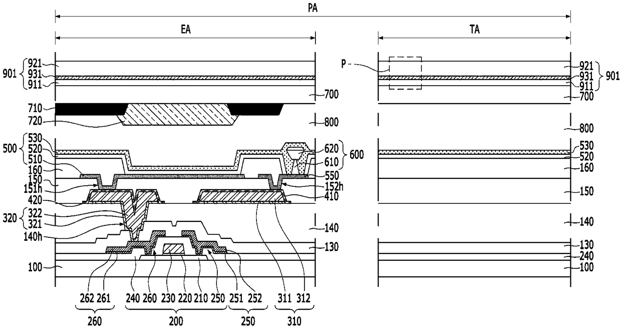
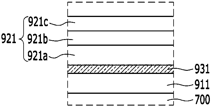
[0035] figure 1 is a diagram schematically illustrating a display device according to an embodiment of the present invention. figure 2 Yes figure 1 Magnified view of region P in .
[0036] refer to figure 1 and 2 , The display device according to the embodiment of the present invention may include a lower substrate 100 , a thin film transistor 200 , a light emitting structure 500 , an upper substrate 700 and an upper AR structure 901 .
[0037] The lower substrate 100 may support the thin film transistor 200 and the light emitting structure 500 . The lower substrate 100 may include an insulating material. The lower substrate 100 may include a transparent material. For example, the lower substrate 100 may include glass or plastic.
[0038] The lower substrate 100 may include a pixel area PA. Each pixel area PA may display a unique color. Adjacent pixel areas PA may display colors different from each other. For example, the lower substrate 100 may include a blue pixel...
PUM
| Property | Measurement | Unit |
|---|---|---|
| thickness | aaaaa | aaaaa |
| thickness | aaaaa | aaaaa |
Abstract
Description
Claims
Application Information


