

Method for fabricating organic optoelectronic devices
- Summary
- Abstract
- Description
- Claims
- Application Information
AI Technical Summary
Benefits of technology
Problems solved by technology
Method used
Image

Examples
Embodiment Construction
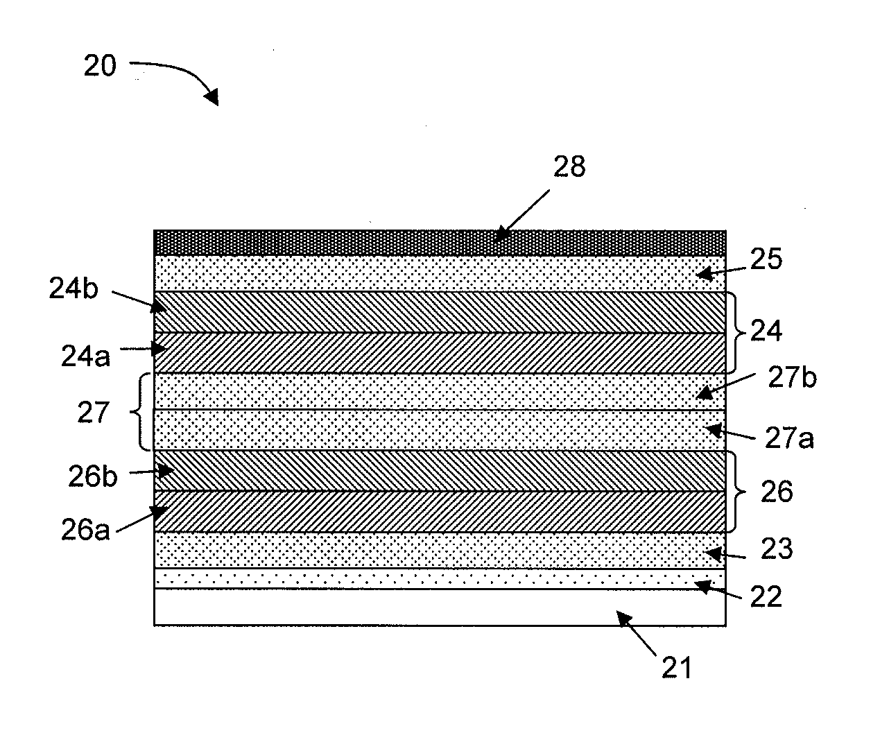
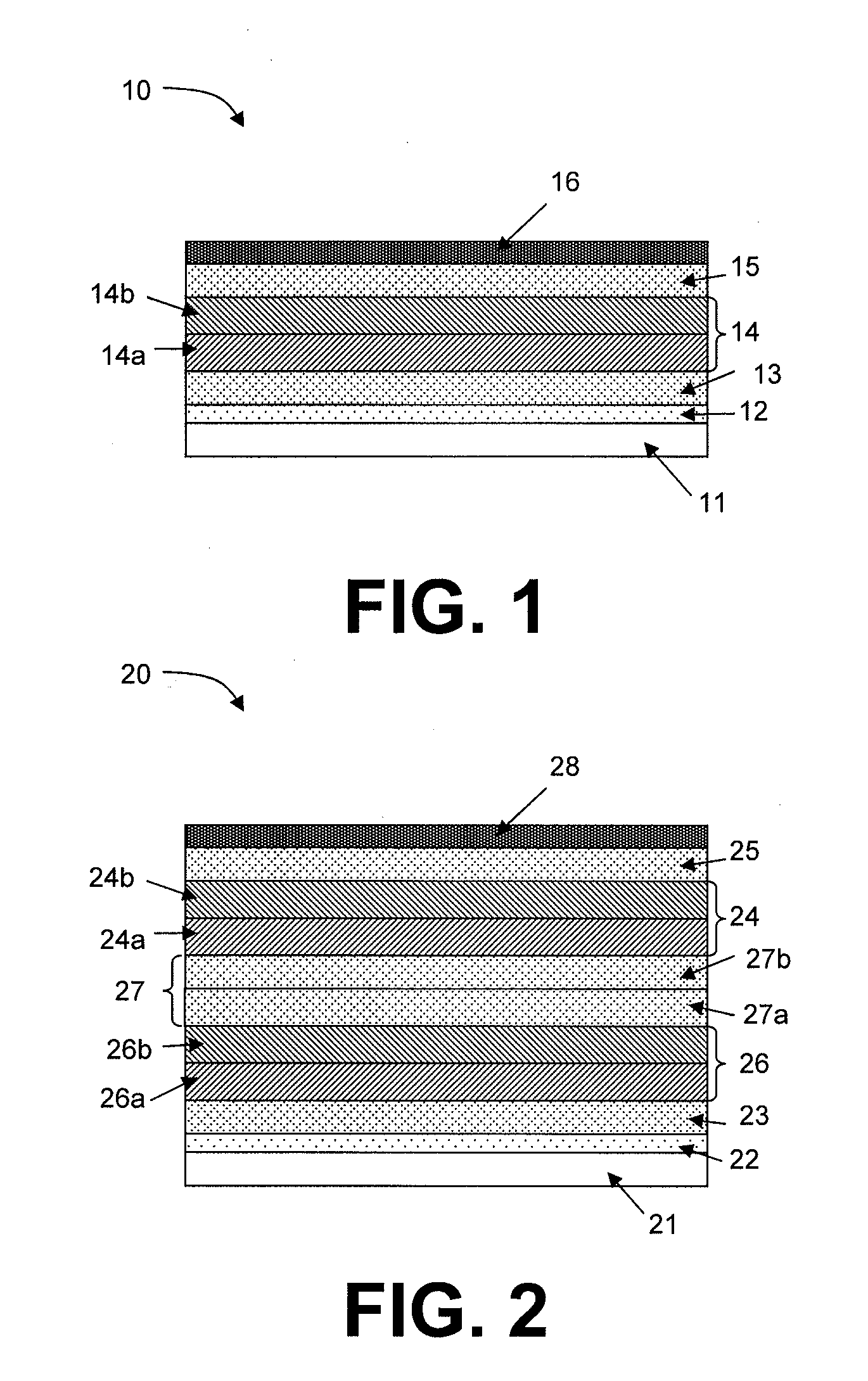
[0012]One aspect relates to optoelectronic devices comprising an intermediate layer which can be simultaneously thick enough to permit good barrier and / or buffer properties, sufficiently transparent to make it suitable for use in a solar cell and sufficiently conducting to keep the series resistance of the device at a low level.
[0013]Certain aspects relate to a method for fabricating organic optoelectronic devices, wherein the method comprises providing at least one metal oxide layer that is optically transparent (e.g. >about 80% in the relevant portion of the spectrum) and has a good electrical conductivity (e.g. an electrical conductivity higher than about 10−5 S / cm, preferably higher than about 10−4 S / cm) and wherein the at least one metal oxide layer can be formed directly on an underlying organic layer, e.g. organic semiconductor layer, with no risk or with a very limited risk of damaging the organic layer, e.g. organic semiconductor layer.
[0014]Certain aspects relate to a meta...
PUM
 Abstract
Description
Claims
Application Information