Printed circuit board processing device

A technology for printed circuit boards and processing devices, which is applied in the direction of printed circuits, printed circuit manufacturing, printing technology, etc., can solve problems affecting production efficiency, circuit board solder paste gaps, circuit board processing failures, etc., to improve production efficiency and improve Printing effect, quality assurance effect

Inactive Publication Date: 2018-07-03
广东高旗技术有限公司
View PDF0 Cites 6 Cited by
  • Summary
  • Abstract
  • Description
  • Claims
  • Application Information

AI Technical Summary

Problems solved by technology

At present, during the solder paste printing process of printed circuit boards, there are often some dust on the surface of printed circuit boards, which affects the printing effect of solder paste, and then affects the quality of printed circuit boards. The lack of complete contact of the boards leads to gaps in the solder paste printed on the circuit boards, which leads to the failure of the circuit board processing and affects the production efficiency. For this reason, we propose a printed circuit board processing device

Method used


Image

  • Printed circuit board processing device
  • Printed circuit board processing device
  • Printed circuit board processing device

Examples


Embodiment Construction

[0014] The following will clearly and completely describe the technical solutions in the embodiments of the present invention with reference to the accompanying drawings in the embodiments of the present invention. Obviously, the described embodiments are only some, not all, embodiments of the present invention. Based on the embodiments of the present invention, all other embodiments obtained by persons of ordinary skill in the art without making creative efforts belong to the protection scope of the present invention.

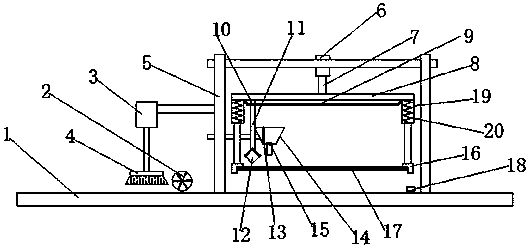
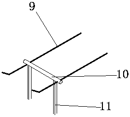
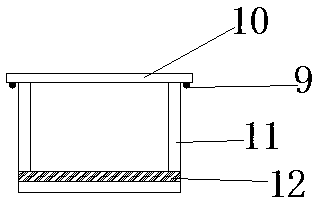
[0015] The present invention provides such Figure 1-3 A kind of printed circuit board processing device shown, comprises conveying table 1, frame 5, slide bar 10, brush block 4, connecting block 16, top plate 8 and rhombus scraper 12, the left side of described frame 5 is fixed with Motor 3, the output shaft of the motor 3 is connected with the brush block 4, the height of the brush of the brush block 4 is 1-2mm lower than the surface height of the circuit bo...


PUM


Abstract

The invention discloses a printed circuit board processing device, which comprises a transfer table, a frame, a sliding rod, a brush block, connecting blocks, a jacking plate and a diamond-shaped scraper, wherein a motor is fixed to the left side of the frame, an output shaft of the motor is in transmission connection with the brush block, the right side of the brush block is provided with a fan,a cylinder is fixed to the top end of the frame, the cylinder is fixedly connected with the jacking plate, the lower surface of the jacking plate is provided with guide rails, the guide rails are slidably connected with the sliding rod, the sliding rod is fixedly connected with the diamond-shaped scraper, elastic telescopic rods are fixed to both sides of the jacking plate, a spring is arranged inside each elastic telescopic rod, the elastic telescopic rods are fixedly connected with a steel mesh by means of the connecting blocks, a sensing device is arranged below one connecting block, a solder paste tank is arranged above the steel mesh, a stirring rod is arranged inside the solder paste tank, and a valve is arranged at the bottom part of the solder paste tank. The printed circuit boardprocessing device ensures the processing effect of a printed circuit board, and improves the production efficiency.

Description

technical field [0001] The invention belongs to the technical field of printed circuit board processing, and in particular relates to a printed circuit board processing device. Background technique [0002] With the development requirements of multi-function, miniaturization and high performance of electronic products, printed circuit boards are developing in the direction of high-level, high-density and thin core boards. In the production process of printed circuit boards, surface assembly technology is an important part of printed circuit board processing technology, and the printing of solder paste is the first process of surface assembly technology, and it is also the most critical process. At present, during the solder paste printing process of printed circuit boards, there are often some dust on the surface of printed circuit boards, which affects the printing effect of solder paste, and then affects the quality of printed circuit boards. The lack of complete contact ...

Claims


Application Information

Patent Timeline
Patent Type & Authority Applications(China)
IPC IPC(8): H05K3/12B41F15/08B41F15/14B41F15/44B41F23/00
CPCH05K3/1233B41F15/08B41F15/14B41F15/44B41F23/002B41P2215/50H05K2203/0139
Inventor 郑晓滨
Owner 广东高旗技术有限公司
Why Eureka
Try Eureka