Thermal bubble ink jet printing head chip and manufacturing method thereof

The technology of an inkjet printing head and its manufacturing method, which is applied in the field of printing, can solve the problems of performance impact, impact on printing quality, high manufacturing cost and use cost of printing equipment, etc.

Inactive Publication Date: 2018-07-06
SHANGHAI AUREFLUIDICS TECH CO LTD
View PDF7 Cites 5 Cited by
  • Summary
  • Abstract
  • Description
  • Claims
  • Application Information

AI Technical Summary

Problems solved by technology

[0003] In order to further increase the integrated printing width of wide-format printing equipment, the print head needs to apply a current of up to several amperes, resulting in a large manufacturing cost and use cost of the printing equipment
In addition, the temperature of the circuit components in the print head will rise rapidly under the action of high current, and the performance will be affected, thereby affecting the printing quality. In order to ensure the printing quality, the print head needs to work periodically

Method used


Image

  • Thermal bubble ink jet printing head chip and manufacturing method thereof
  • Thermal bubble ink jet printing head chip and manufacturing method thereof
  • Thermal bubble ink jet printing head chip and manufacturing method thereof

Examples


Embodiment 1

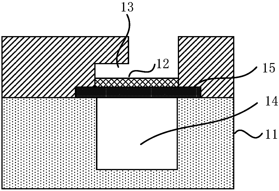
[0038] figure 1 It is a schematic structural diagram of a thermal bubble jet print head chip provided by Embodiment 1 of the present invention. refer to figure 1 , the print head chip includes a substrate 11 , a heating resistor 12 , an ink containing cavity 13 and a low thermal conductivity cavity 14 . Wherein, a heating resistor 12 is formed on the first side of the substrate 11, and an ink containing cavity 13 is formed on the side of the heating resistor 12 away from the substrate 11; wherein, a low thermal conductivity cavity 14 is formed in the substrate 11, and the low thermal conductivity cavity 14 is located on the side of the heating resistor 12 away from the ink containing cavity 13 , and the low thermal conductivity cavity 14 is filled with a material with lower thermal conductivity than the substrate. Specifically, by forming a low thermal conductivity cavity 14 in the substrate 11 and filling the low thermal conductivity cavity 14 with a material with a thermal...

Embodiment 2

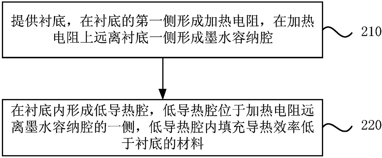
[0044] image 3It is a method for manufacturing a thermal bubble inkjet print head chip provided in Embodiment 2 of the present invention, and the method is suitable for reducing heat loss of heating resistors and improving heating efficiency. The method can be executed by a thermal bubble jet print head chip configured in the printer.

[0045] refer to image 3 , the manufacturing method of the thermal bubble inkjet printing head chip that the present embodiment provides, specifically comprises the following steps:

[0046] Step 210 , providing a substrate, forming a heating resistor on a first side of the substrate, and forming an ink containing chamber on a side of the heating resistor away from the substrate.

[0047] After the substrate is provided, a heating resistor is formed on the first side of the substrate for generating heat, and an ink containing chamber is formed on the side of the heating resistor away from the substrate for storing ink. When the heat generat...

Embodiment 3

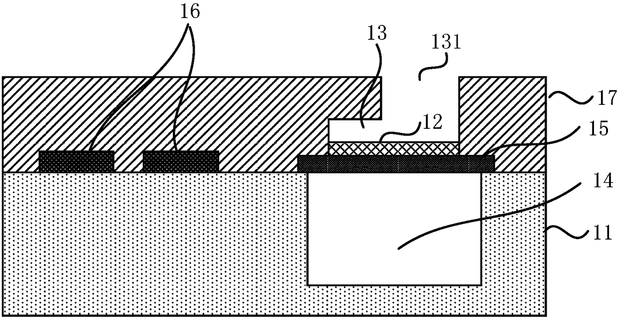
[0052] Figure 4 It is a method for manufacturing a thermal bubble jet print head chip provided in Embodiment 3 of the present invention, refer to Figure 4 , on the basis of the above embodiment, the forming the low thermal conductivity cavity in the substrate includes: forming at least two micro cavities on the second side surface of the substrate; forming a low thermal conductivity cavity in the substrate through at least two micro cavities Thermal cavity. That is, step 220 in the second embodiment includes the following steps 320 and 330 .

[0053] refer to Figure 4 , the manufacturing method of the thermal bubble inkjet print head chip of the present embodiment specifically includes:

[0054] Step 310 , providing a substrate, forming a heating resistor on a first side of the substrate, and forming an ink containing cavity on a side of the heating resistor away from the substrate. For details, please refer to the description in step 210 in the second embodiment.

[0...


PUM


Abstract

The embodiment of the invention provides a thermal bubble ink jet printing head chip and a manufacturing method of the thermal bubble ink jet printing head chip and relative to the technical field ofprinting. The thermal bubble ink jet printing head chip comprises a substrate and a heating resistor formed on the first side of the substrate. The side, far away from the substrate, of the heating resistor is provided with an ink containing cavity. A low-heat-conductivity cavity is formed in the substrate and located on the side, far away from the ink containing cavity, of the heating resistor. Amaterial with the heat conductivity lower than that of the substrate is fed in the low-heat-conductivity cavity. Diffusion of the heat generated by the heating resistor to the substrate is correspondingly reduced by the adoption of the low-heat-conductivity cavity, namely the heat is kept in the ink containing cavity, and the heating efficiency of the heating resistor is improved; in this way, the work current of the heating resistor can be correspondingly lowered, the integrated print wide format of digital wide-format print equipment is improved, meanwhile the work current of a printing head and the temperature rising rate of the substrate are reduced, and therefore the printing speed of the high-speed digital wide-format print equipment is improved.

Description

technical field [0001] The embodiments of the present invention relate to the field of printing technology, and in particular to a thermal bubble jet printing head chip and a manufacturing method thereof. Background technique [0002] The thermal bubble jet print head chip of high-speed digital wide-format printing equipment has the advantages of mass production, high resolution, and low cost, and is widely used. Its working principle is that the tiny resistance of the thermal bubble inkjet print head chip will generate a large amount of heat in a very short time under the action of a large current, causing the ink in the resistance area to vaporize instantly to form bubbles and expand rapidly, forcing the ink to be ejected. [0003] In order to further increase the integrated printing width of the wide-format printing device, the print head needs to apply a current up to several amperes, which results in a high manufacturing cost and usage cost of the printing device. In a...

Claims


Application Information

Patent Timeline
Patent Type & Authority Applications(China)
IPC IPC(8): B41J2/14B41J2/16
CPCB41J2/14129B41J2/1601B41J2/1603B41J2/1628B41J2/1408B41J2/14112B41J2/1606B41J2/1626
Inventor 关一民王小伟张华
Owner SHANGHAI AUREFLUIDICS TECH CO LTD
Why Eureka
Try Eureka