GaN HEMT accelerated life test method

An accelerated life test and life test technology, applied in the direction of measuring devices, instruments, scientific instruments, etc., can solve the problem of low reliability of GaNHEMT accelerated life test, and achieve the effect of improving the reliability

Active Publication Date: 2018-07-27
河北中瓷电子科技股份有限公司石家庄高新区分公司
View PDF10 Cites 2 Cited by
  • Summary
  • Abstract
  • Description
  • Claims
  • Application Information

AI Technical Summary

Problems solved by technology

[0004] In view of this, an embodiment of the present invention provides a GaN HEMT accelerated life test method, by using the same test station, different test temperature change temperature test groups, and comparing the test results with multiple fixed temperature test groups to solve the problem. The problem of low reliability of GaN HEMT accelerated life test using the accelerated life test method of microelectronic devices in the prior art

Method used


Image

  • GaN HEMT accelerated life test method

Examples


Embodiment Construction

[0042] In the following description, specific details such as specific system structures and technologies are presented for the purpose of illustration rather than limitation, so as to thoroughly understand the embodiments of the present invention. It will be apparent, however, to one skilled in the art that the invention may be practiced in other embodiments without these specific details. In other instances, detailed descriptions of well-known systems, devices, circuits, and methods are omitted so as not to obscure the description of the present invention with unnecessary detail.

[0043] In order to illustrate the technical solutions of the present invention, specific examples are used below to illustrate.

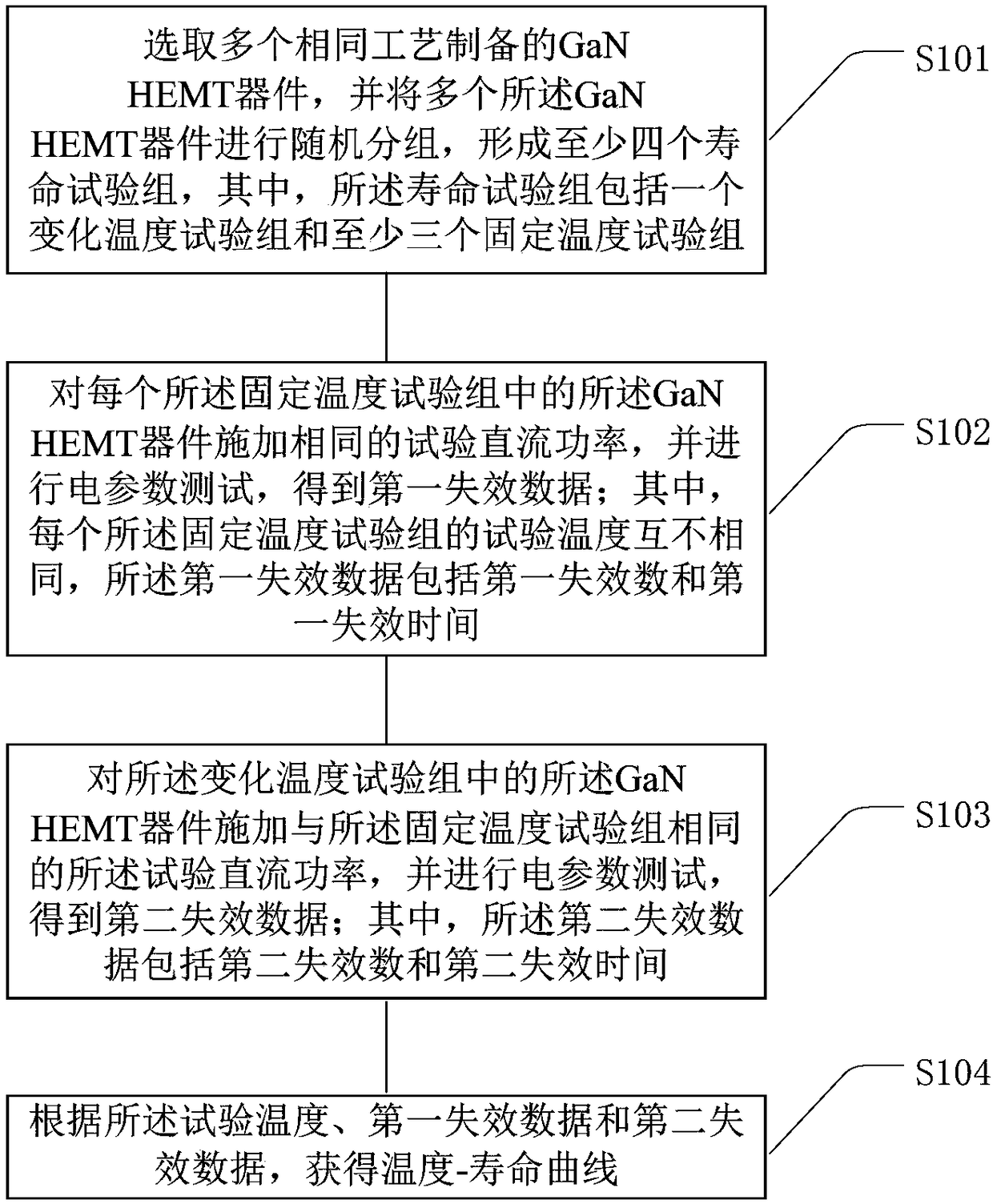
[0044] Please refer to figure 1 , GaN HEMT accelerated life test method, including:

[0045] Step S101, selecting a plurality of GaN HEMT devices prepared by the same process, and randomly grouping the plurality of GaN HEMT devices to form at least four life test grou...


PUM


Abstract

The invention is suitable for the technical field of semiconductors, and provides a GaN HEMT accelerated life test method. The method comprises the following steps: selecting a plurality of GaN HEMT devices prepared in a same process, randomly grouping the plurality of GaN HEMT devices, and forming at least four service life test groups, wherein each service life test group comprises a variation temperature test group and at least three fixed temperature test groups; applying the same test DC power to the GaN HEMT device in each fixed temperature test group, testing electric parameters, and obtaining first failure data; applying the same test DC power with the fixed temperature test group to the GaN HEMT device in the variation temperature test group, testing the electric parameters, and obtaining second failure data; and obtaining a temperature-service life curve according to the test temperature, the first failure data and the second failure data. By adopting the GaN HEMT acceleratedlife test method, the consistence of the GaN HEMT accelerated life test can be verified, and the test credibility is improved.

Description

technical field [0001] The invention belongs to the technical field of semiconductors, in particular to a GaN HEMT accelerated life test method. Background technique [0002] The lifetime of microelectronic devices is a reliability indicator that device manufacturers or users are very concerned about. Since GaN high electron mobility transistors (High Electron Mobility Transistor, HEMT) are devices developed using third-generation semiconductor materials, if conventional If the reliability test method of silicon or gallium arsenide devices is used to estimate the life of gallium nitride devices, the test time will be too long, which will lead to more external interference factors and have a negative impact on the test results; or due to improper selection of test conditions, it is very easy to Doubts about the reliability of the test results. [0003] At present, the accelerated life test of microelectronic devices uses DC power or radio frequency accelerated life test as t...

Claims


Application Information

Patent Timeline
Patent Type & Authority Applications(China)
IPC IPC(8): G01N25/00
CPCG01N25/00
Inventor 潘宏菽宋建博杨中月崔玉兴
Owner 河北中瓷电子科技股份有限公司石家庄高新区分公司
Why Eureka
Try Eureka