
Eureka
For R&D, Eureka makes reading and utilizing patents & technical documents easy.
Eureka AIR
Designed for self-driven R&D workflows. Generate viable solutions, solve complex R&D challenges, empower your innovation with AI.

Eureka Materials
Designed for material experts only. Revolutionize your material R&D, from search, analyze, to developing new materials.

TechResearch
Generate reliable direction feasibility study reports for your R&D in just a few steps.

TechSeek
Discover and master advanced knowledge NOW. Basics, ideas, possibilities, all at once.

TechMind
As an expert in R&D Theories, TechMind can generates customized viable solutions instantly.

TechRisk
Analyze your overall solution with one click, know your potential R&D risks in advance.

TechMonitor
Get weekly tech updates, stay abreast of the latest tech innovations and key insights.
Connecting bar
A technology of connecting strips and strips, which is applied in the field of connecting strips and can solve problems such as SOI integrated circuit defects
- Summary
- Abstract
- Description
- Claims
- Application Information
AI Technical Summary
Problems solved by technology
Method used
Image

Examples
Embodiment Construction
[0020] Like elements are referenced by like reference numerals in the various figures, and furthermore, the various views are not drawn to scale. For the sake of clarity, only those elements that are useful to the understanding of the described embodiments are shown and are shown in detail.
[0021] In the following description, when referring to positional descriptions such as the terms "front", "above", "upper", etc. or orientation descriptions such as the term "vertical", the references made are based on the elements discussed in the drawings. position.
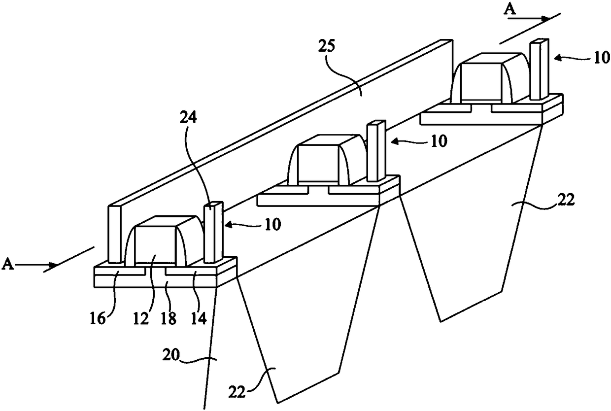
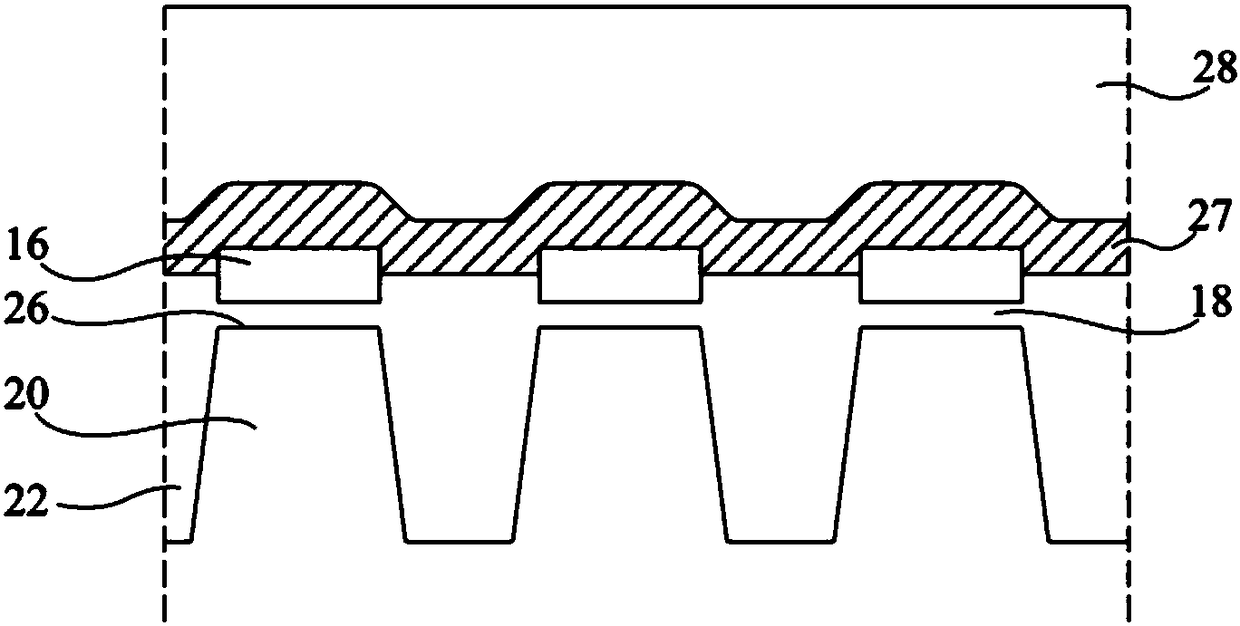
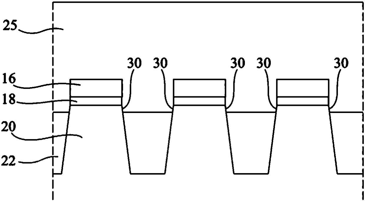
[0022] figure 1 is a partial schematic perspective view of three transistors 10 formed in and on a thin silicon-on-insulator (SOI) layer. Each transistor is formed in and on an active region defined in a thin silicon layer. Each transistor includes a gate 12 , a drain region 14 and a source region 16 . Each active area is located on an insulator layer 18 called BOX (for buried oxide), usually made of silicon dioxide. ...
PUM
 Abstract
Description
Claims
Application Information
 - R&D Engineer
- R&D Manager
- IP Professional
- Industry Leading Data Capabilities
- Powerful AI technology
- Patent DNA Extraction
Browse by: Latest US Patents, China's latest patents, Technical Efficacy Thesaurus, Application Domain, Technology Topic, Popular Technical Reports.
© 2024 PatSnap. All rights reserved.Legal|Privacy policy|Modern Slavery Act Transparency Statement|Sitemap|About US| Contact US: help@patsnap.com