Film-making method and film-forming device

A film-forming device and thin-film technology, which is applied in the direction of metal material coating process, coating, gaseous chemical plating, etc., can solve the problems of deterioration of film-forming plasma distribution, affecting the quality of thin-film transistors, and poor film-forming uniformity

Active Publication Date: 2020-06-30
TRULY HUIZHOU SMART DISPLAY
View PDF9 Cites 0 Cited by
  • Summary
  • Abstract
  • Description
  • Claims
  • Application Information

AI Technical Summary

Problems solved by technology

However, due to changes in the equipment chamber environment, component differences, component aging and other factors, it will have a local deterioration of the distribution of the film-forming plasma, especially in the edge region of the film, which will lead to the deterioration of the in-plane film-forming uniformity , affecting the quality of thin film transistors

Method used


Image

  • Film-making method and film-forming device
  • Film-making method and film-forming device
  • Film-making method and film-forming device

Examples


Embodiment Construction

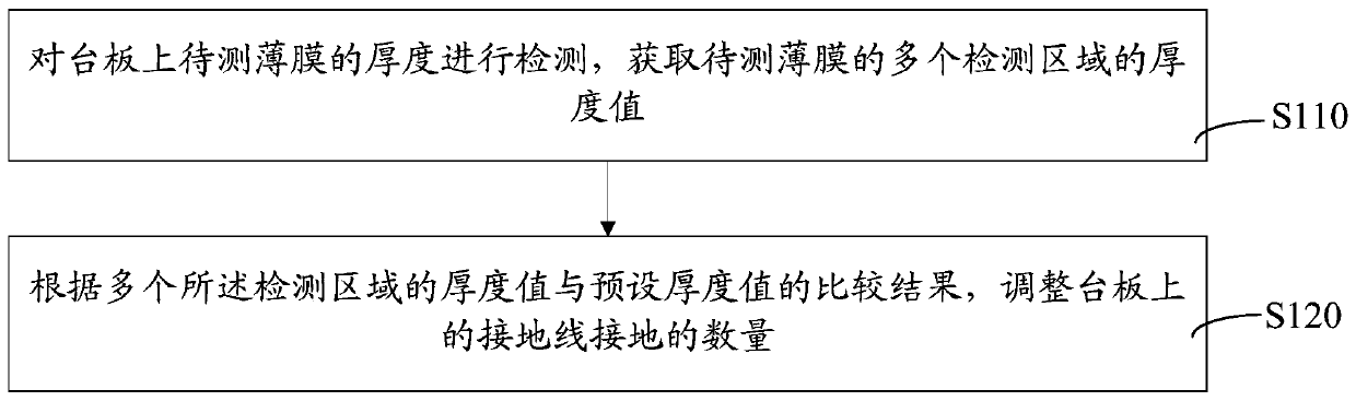
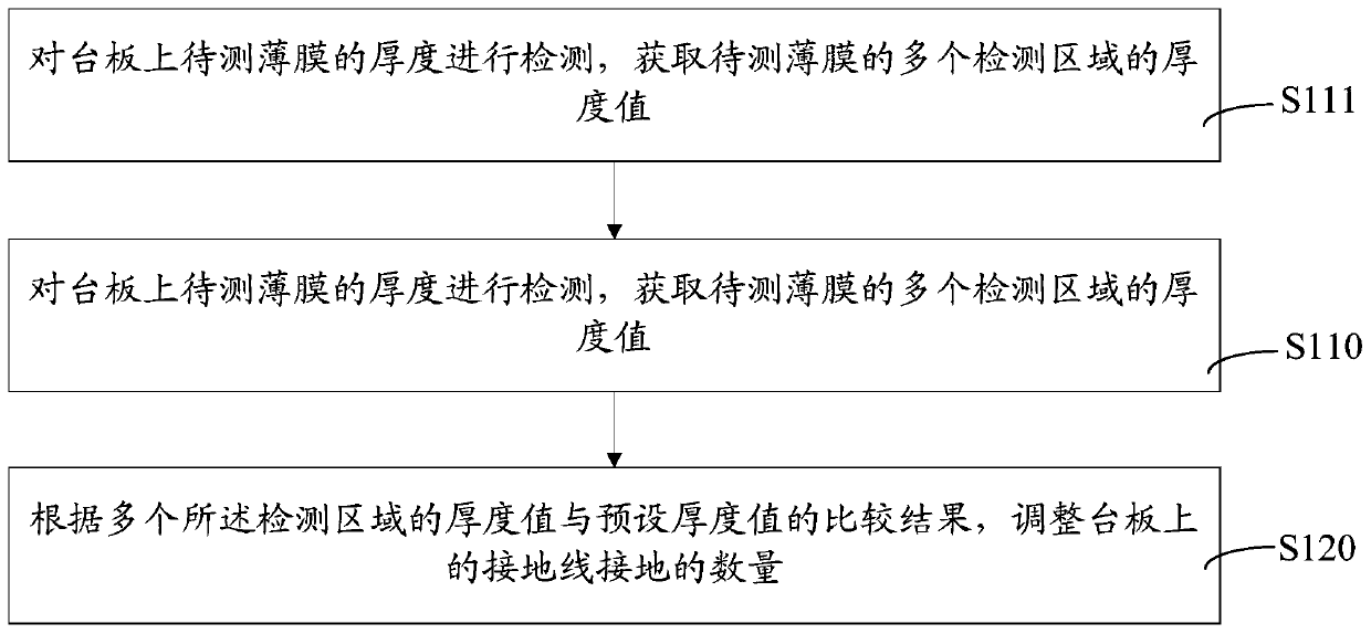
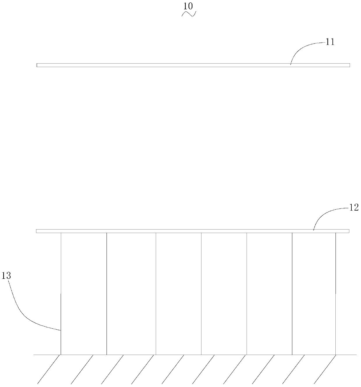
[0021] In order to make the above objects, features and advantages of the present invention more comprehensible, specific implementations of the present invention will be described in detail below in conjunction with the accompanying drawings. In the following description, numerous specific details are set forth in order to provide a thorough understanding of the present invention. However, the present invention can be implemented in many other ways different from those described here, and those skilled in the art can make similar improvements without departing from the connotation of the present invention, so the present invention is not limited by the specific implementations disclosed below.

[0022] It should be noted that when an element is referred to as being “disposed on” another element, it may be directly on the other element or there may also be an intervening element. When an element is referred to as being "connected to" another element, it can be directly connect...


PUM


Abstract

The invention relates to a film making method and a film forming device adopting the film making method. The film making method comprises the steps that the thickness of a to-be-measured thin film iscompared with the preset thickness through the film making method to judge whether the thickness of the formed thin film is consistent with the expected thickness of the thin film or not, so that adjusting grounding wires in a test area and adjusting the thickness during plasma forming the thin film on a table plate are determined, and by adjusting the number of the grounding wires and changing the charge amount guided away by the plasma, the obtained thickness of the thin film is matched with the preset thickness. As for the film forming device, devices for being movably connected with the grounding wires are arranged on the table plate and a metal frame, so that forming of the thin film is smoother, namely, the uniformity of the thin film is high, and the quality of a thin film transistor is improved; and in this way, the problem of local anomaly of film-forming plasma distribution due to the factors such as change of the equipment chamber environment, difference of parts and aging of the parts can be effectively solved, the uniformity of film forming is improved accordingly, and the quality of the thin film transistor is improved.

Description

technical field [0001] The present invention relates to the technical field of thin film transistors, in particular to a film forming method and a film forming device adopting the above film forming method. Background technique [0002] With the development of liquid crystal display screens, the demand for ultra-thin, light-weight, and low-power screens has been continuously raised. The production level of thin film transistors directly determines the quality of display screens. During the manufacturing process of the thin film transistor, the quality of the CVD (Chemical Vapor Deposition, chemical vapor deposition) film has a direct impact on the quality of the thin film transistor. Among them, PECVD (Plasma Enhanced Chemical Vapor Deposition, Plasma Enhanced Chemical Vapor Deposition) is a commonly used film forming method, which uses microwave or radio frequency to ionize the gas containing the constituent atoms of the film to form plasma locally, and the plasma The chem...

Claims


Application Information

Patent Timeline
Patent Type & Authority Patents(China)
IPC IPC(8): C23C16/52C23C16/505
CPCC23C16/505C23C16/52
Inventor 辛少强谢志强任思雨苏君海李建华
Owner TRULY HUIZHOU SMART DISPLAY
Why Eureka
Try Eureka