Multilayer printed wiring board and method for manufacturing multilayer printed wiring board

A multi-layer printing and manufacturing method technology, applied in the field of multi-layer printed circuit board and multi-layer printed circuit board manufacturing, can solve the problems of printed circuit board warpage and other problems, and achieve the effect of flat formation

Active Publication Date: 2013-11-06
IBIDEN CO LTD
View PDF6 Cites 0 Cited by
  • Summary
  • Abstract
  • Description
  • Claims
  • Application Information

AI Technical Summary

Problems solved by technology

As a result, the printed wiring board may be warped during the repeated heat cycle in which the IC chip heats up and then returns to normal temperature.

Method used


Image

  • Multilayer printed wiring board and method for manufacturing multilayer printed wiring board
  • Multilayer printed wiring board and method for manufacturing multilayer printed wiring board
  • Multilayer printed wiring board and method for manufacturing multilayer printed wiring board

Examples


no. 1 example

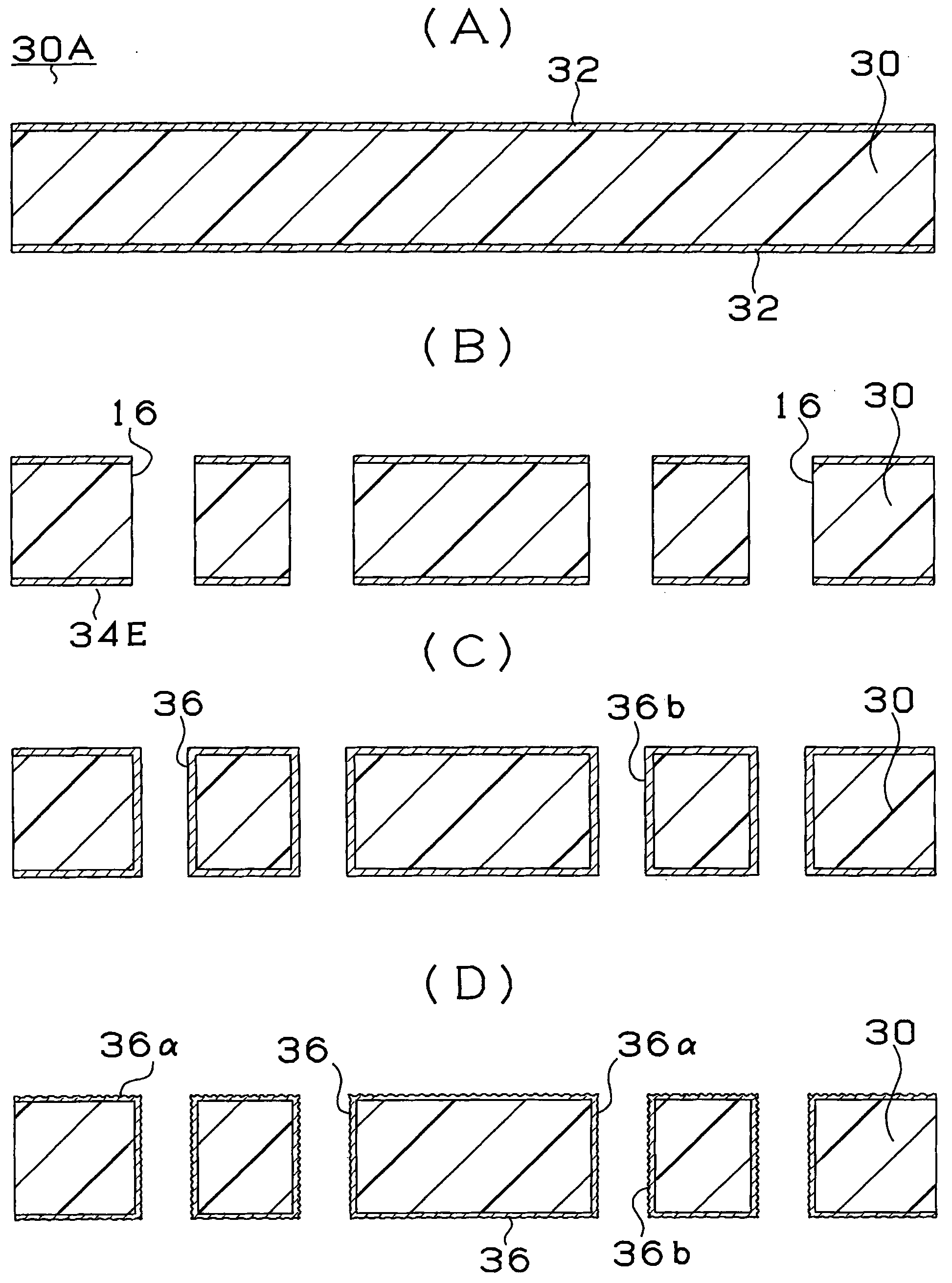
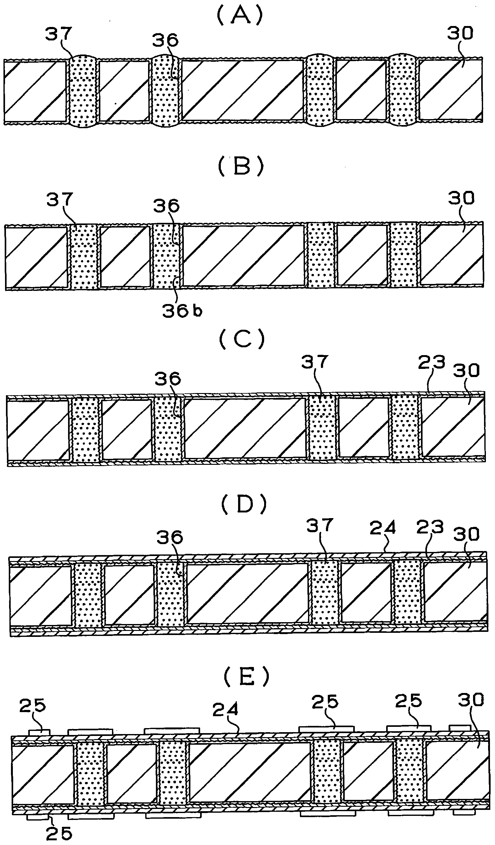
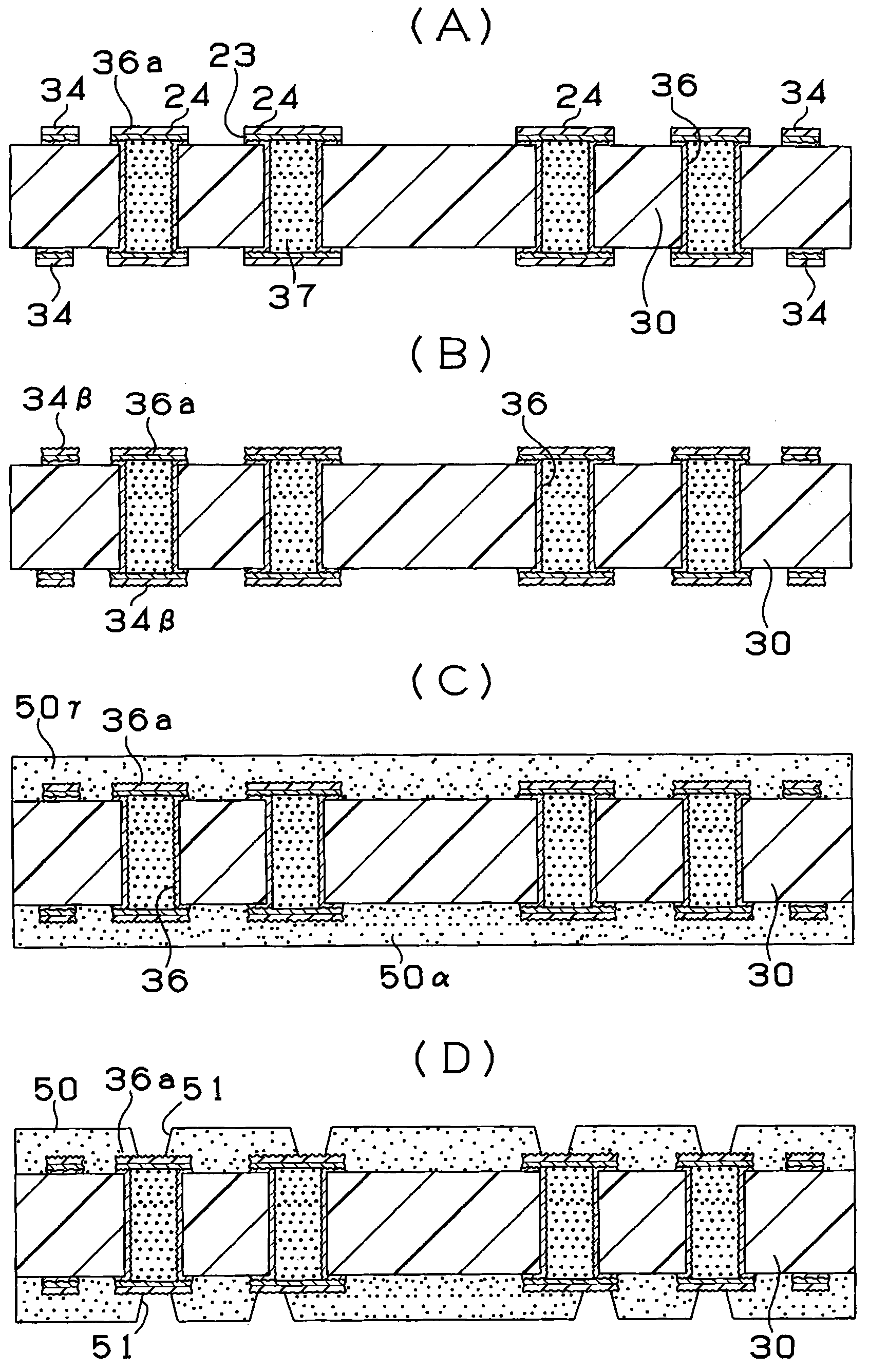
[0045] First, refer to Figure 1 to Figure 10 The structure of the multilayer printed wiring board 10 of the first embodiment of the present invention will be described. Figure 8 A sectional view showing the multilayer printed wiring board 10, Figure 9 expressed in Figure 8 The multilayer printed wiring board 10 is shown in a state where an IC chip 90 is mounted on a daughter board 94 . Figure 10 (B) means Figure 8 b-b cross-section in . Such as Figure 8 As shown, in the multilayer printed wiring board 10 , the conductive circuit 34 is formed on the surface of the core substrate 30 . The surface and the inside of the core substrate 30 are connected by through holes 36 . The via hole 36 is composed of a sidewall conductor layer 36b and a cover plating layer 36a constituting a via land, and the inside of the sidewall conductor layer 36b is filled with a resin filler 37 . Only copper may be filled without filling the resin filler. On the cover plating layer (via-hol...

no. 2 example

[0123] Next, refer to Figure 18 A method of manufacturing a multilayer printed wiring board according to a second embodiment of the present invention will be described.

[0124] In the first embodiment, the recesses for forming conductor circuits and the recesses for forming planar conductors were formed in the interlayer insulating layer by laser light. On the other hand, in the second embodiment, the concave portion for forming a conductive circuit and the concave portion for forming a planar conductor are formed by exposure and development.

[0125] refer to Figure 1 to Figure 5 In (B), the interlayer resin insulating layer 150 is formed in the same manner as in the first embodiment described above. The interlaminar resin insulating layer 150 is made of photosensitive resin (refer to Figure 18 (A)). After placing a mask having a pattern of a conductive circuit and a planar conductor on the interlayer resin insulating layer 150 for exposure, a development treatment is...

no. 3 Embodiment

[0127] Next, refer to Figure 19 A method of manufacturing a multilayer printed wiring board according to a third embodiment of the present invention will be described.

[0128] In the first embodiment, the recesses for forming conductor circuits and the recesses for forming planar conductors were formed in the interlayer insulating layer by laser light. In contrast, in the third embodiment, the conductive circuit forming recesses and the planar conductor forming recesses were formed using a mold (imprint method).

[0129] refer to Figure 1 to Figure 5 In (B), the interlayer resin insulating layer 150 is formed in the same manner as in the first embodiment described above. And, the molding die 210 formed with patterns for forming conductor circuits, planar conductors, and via holes is positioned at a predetermined position (refer to Figure 19 (A)). The molding die 210 is crimped to the interlaminar resin insulating layer 150 (refer to Figure 19 (B)). Then, the molding...


PUM

PropertyMeasurementUnit
thicknessaaaaaaaaaa
thicknessaaaaaaaaaa
current densityaaaaaaaaaa

Abstract

The present invention provides a multi-layer printed wiring board and a manufacturing method of the multi-layer printed wiring board. This method can form a planar layer flat. The convex part (150a) is formed in the concave part (153a) for planar conductor formation of the upper interlaminar resin insulating layer (150). Therefore, when copper plating is filled into the concave portion (153a) for forming a planar conductor, copper can be deposited not only on the sidewall and bottom surface of the concave portion (153a), but also on the surrounding sidewall of the convex portion (150a). . Thereby, the planar layer (159) can be formed flat.

Description

technical field [0001] The present invention relates to a build-up multilayer printed wiring board and a method for manufacturing the multilayer printed wiring board, in particular to a multilayer printed wiring board having a plain conductor and a method for manufacturing the multilayer printed wiring board. Background technique [0002] In printed wiring boards constituting package substrates for mounting electronic components such as IC chips, a fine pitch circuit structure is required as IC chips become more functional. In order to realize a fine pitch, it has been proposed not to form a circuit by the conventional additive method, but to form a circuit using a laser as shown in Patent Document 1. In the operation of this circuit formation, such as Figure 28 As shown in (B), using the laser in the Figure 28 In the interlaminar resin insulating layer 350 shown in (A), a recess 353b for circuit formation, an opening 351 for forming a via conductor, and a recess 353a for ...

Claims


Application Information

Patent Timeline
Patent Type & Authority Patents(China)
IPC IPC(8): H05K3/46H05K3/22
CPCH01L23/49822H01L23/49827H01L23/49838H01L2221/68345H01L2224/16H01L2924/01004H01L2924/01046H01L2924/01078H01L2924/01079H01L2924/15174H01L2924/15311H01L2924/3011H05K2201/0373H05K2201/0949H05K2201/09736H05K2201/10674H01L2224/16225H01L2924/01019H01L2224/05573H01L2224/05568H01L2924/00014H01L2224/0554H05K3/465Y10T29/4913Y10T29/49156Y10T29/49128Y10T29/49165Y10T29/49126Y10T29/49155H01L2224/05599H01L2224/0555H01L2224/0556
Inventor 竹中芳纪中村武志
Owner IBIDEN CO LTD
Why Eureka
Try Eureka