

Wiring substrate, process for manufacturing the wiring substrate, and carrier sheet for green sheet used in the manufacturing process
a manufacturing process and wiring substrate technology, applied in the field of wiring substrates, can solve the problems of deformation of the foil, deterioration of the flatness of the adjoining green sheet, and inability to restore the original mode, so as to reduce the protrusion, and prevent the formation of clearances
- Summary
- Abstract
- Description
- Claims
- Application Information
AI Technical Summary
Benefits of technology
Problems solved by technology
Method used
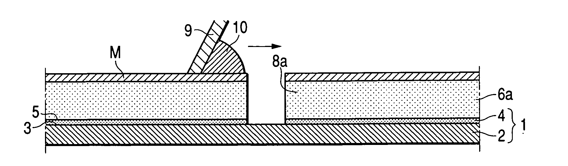
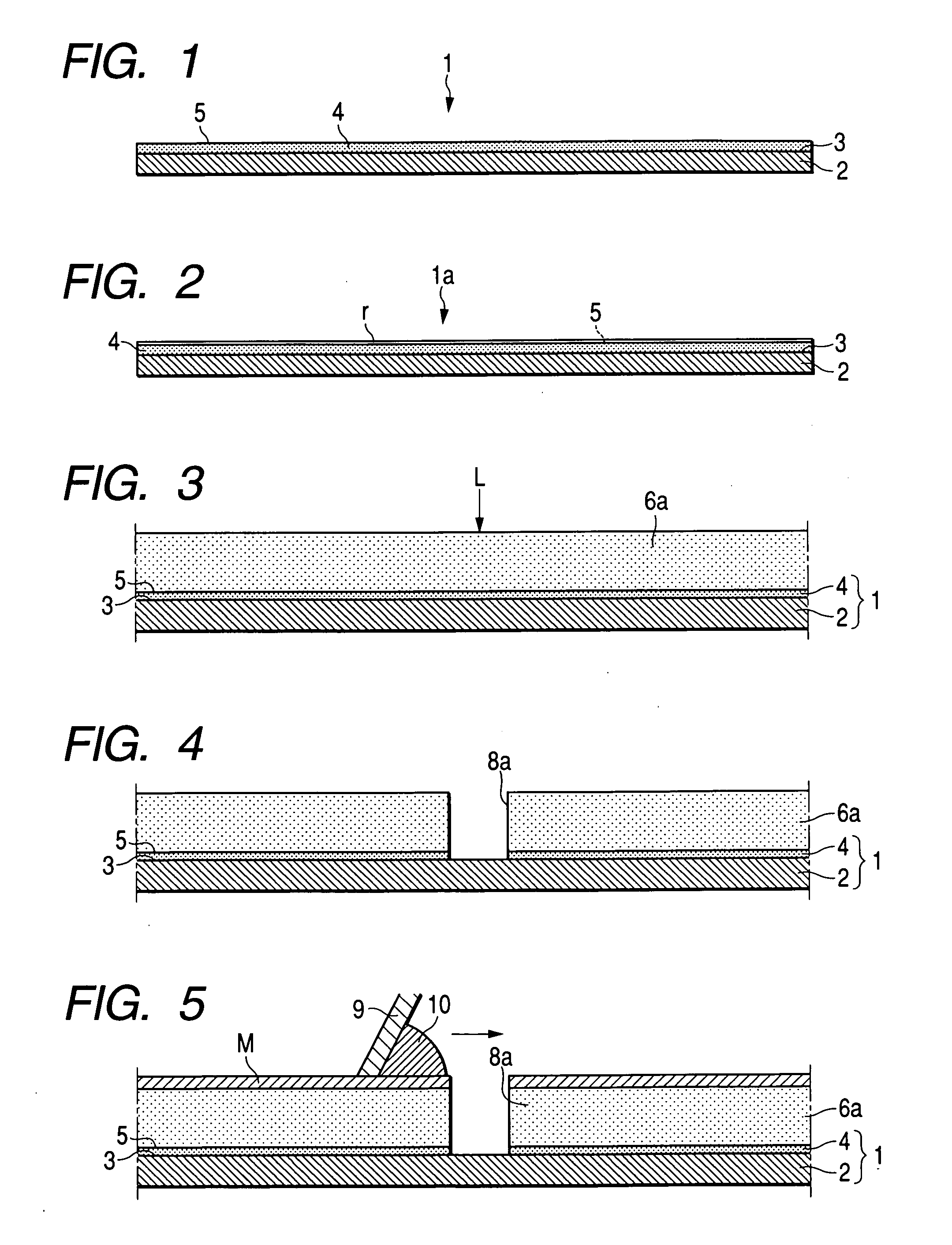
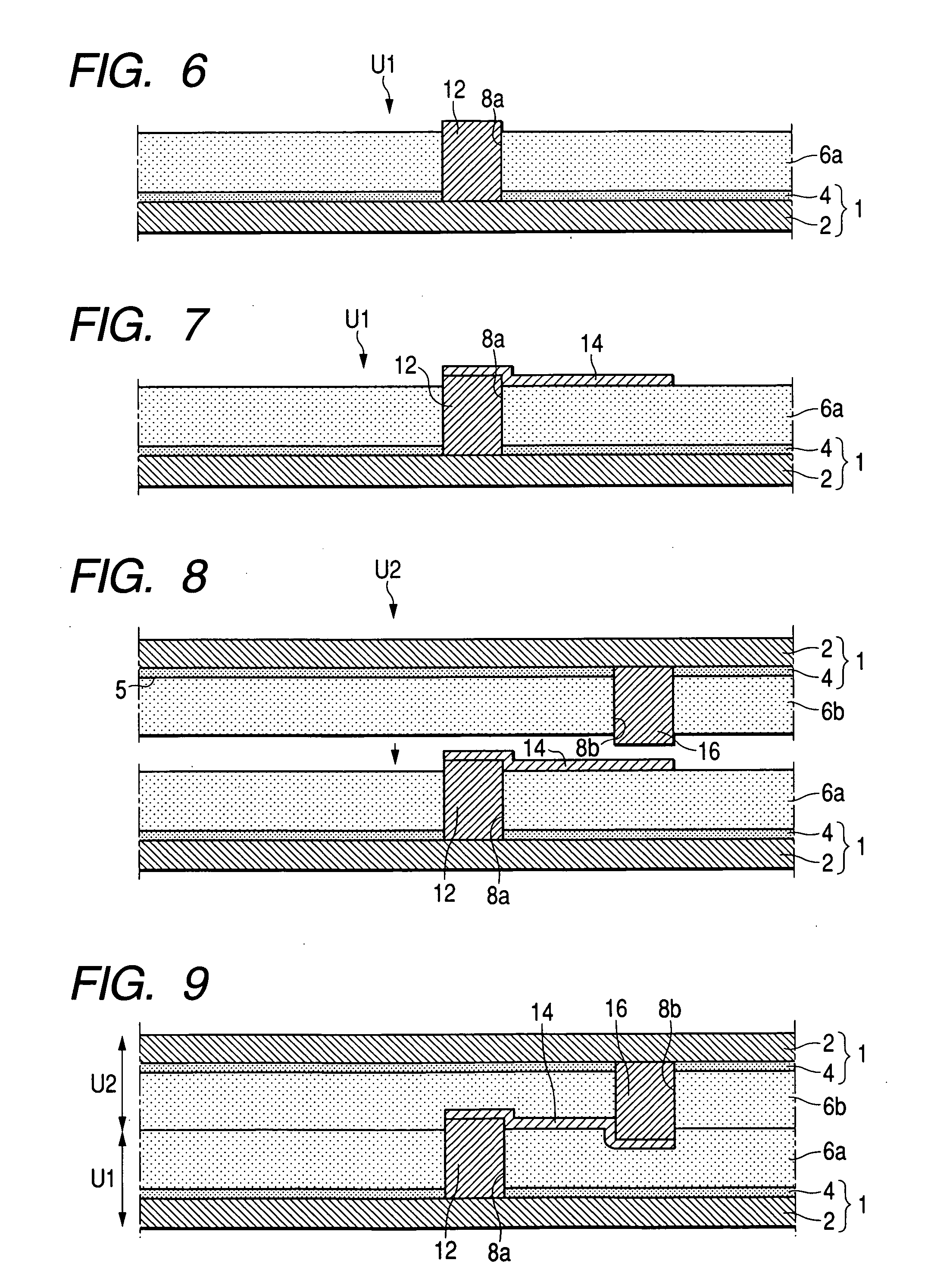
Image

Examples
examples
[0131] Here will be described Specific Examples of the wiring substrate K′.
[0132] Twelve wiring substrates K′ of the structure thus far described were manufactured by the aforementioned manufacturing process using the carrier sheet 1b and changing the thicknesses of the insulating layers s1 to s3. Moreover, six wiring substrates of the aforementioned structure were manufactured by the similar manufacturing process using the carrier sheet of the prior art made exclusively of the PET film and by changing the thicknesses of the insulating layers s1 to s3.
[0133] The twelve wiring substrates K′ were manufactured by changing the thickness of the PET film (or the resin film) 4 while keeping the aluminum foil 2 of the carrier sheet 1b at a constant thickness of 30 μm.
[0134] On the totally eighteen wiring substrates (K′), individually, the ratio t1 / t2 of the thickness t1 of the insulating layer s2, as sandwiched between the protrusions 35 and 37 and between the wiring layers 34 and 36, to...
PUM
| Property | Measurement | Unit |
|---|---|---|
| Length | aaaaa | aaaaa |
| Depth | aaaaa | aaaaa |
| Thickness | aaaaa | aaaaa |
Abstract
Description
Claims
Application Information