Connection device of ceramic antenna and printed circuit board

A printed circuit board, ceramic antenna technology, applied in the direction of antenna support/installation device, conductive connection, electrical component connection, etc., can solve problems such as antenna interference, achieve the effect of eliminating shielding and improving flexibility

Inactive Publication Date: 2018-08-07
南京舒尔斯科技有限公司
View PDF2 Cites 0 Cited by
  • Summary
  • Abstract
  • Description
  • Claims
  • Application Information

AI Technical Summary

Problems solved by technology

However, the metal shell will cause interference to the antenna built in the shell, so that the signal cannot be transmitted through the metal shell

Method used


Image

  • Connection device of ceramic antenna and printed circuit board
  • Connection device of ceramic antenna and printed circuit board
  • Connection device of ceramic antenna and printed circuit board

Examples


no. 1 example

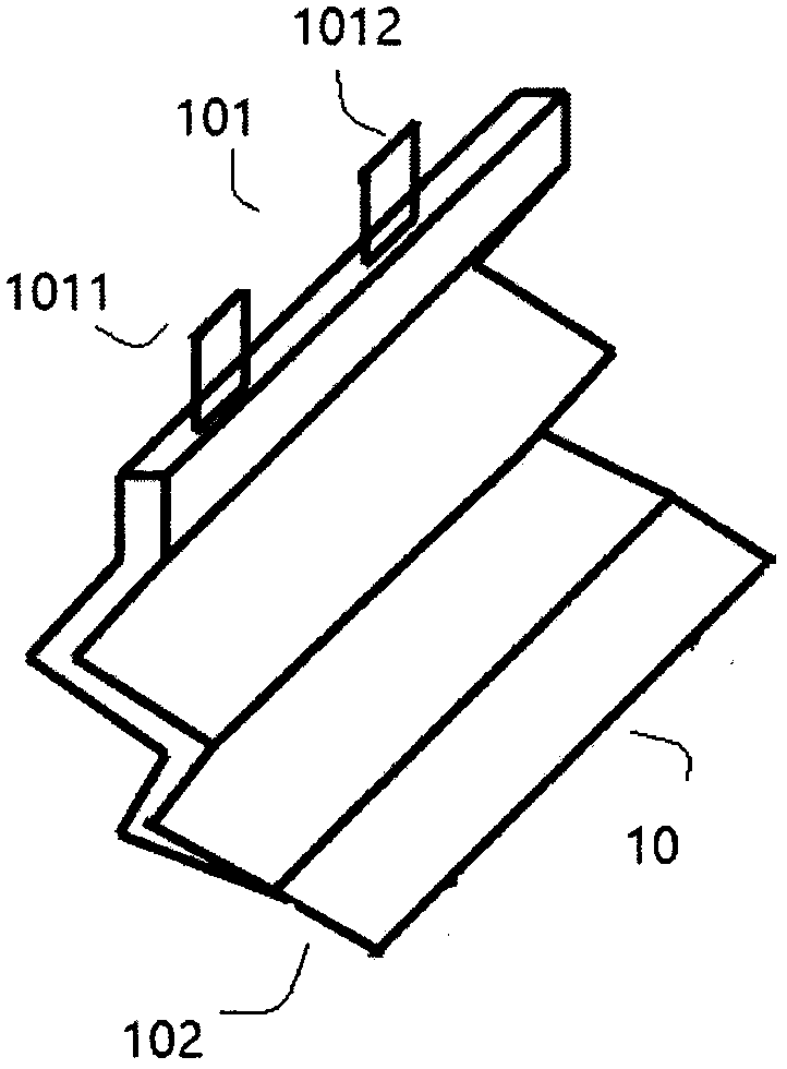
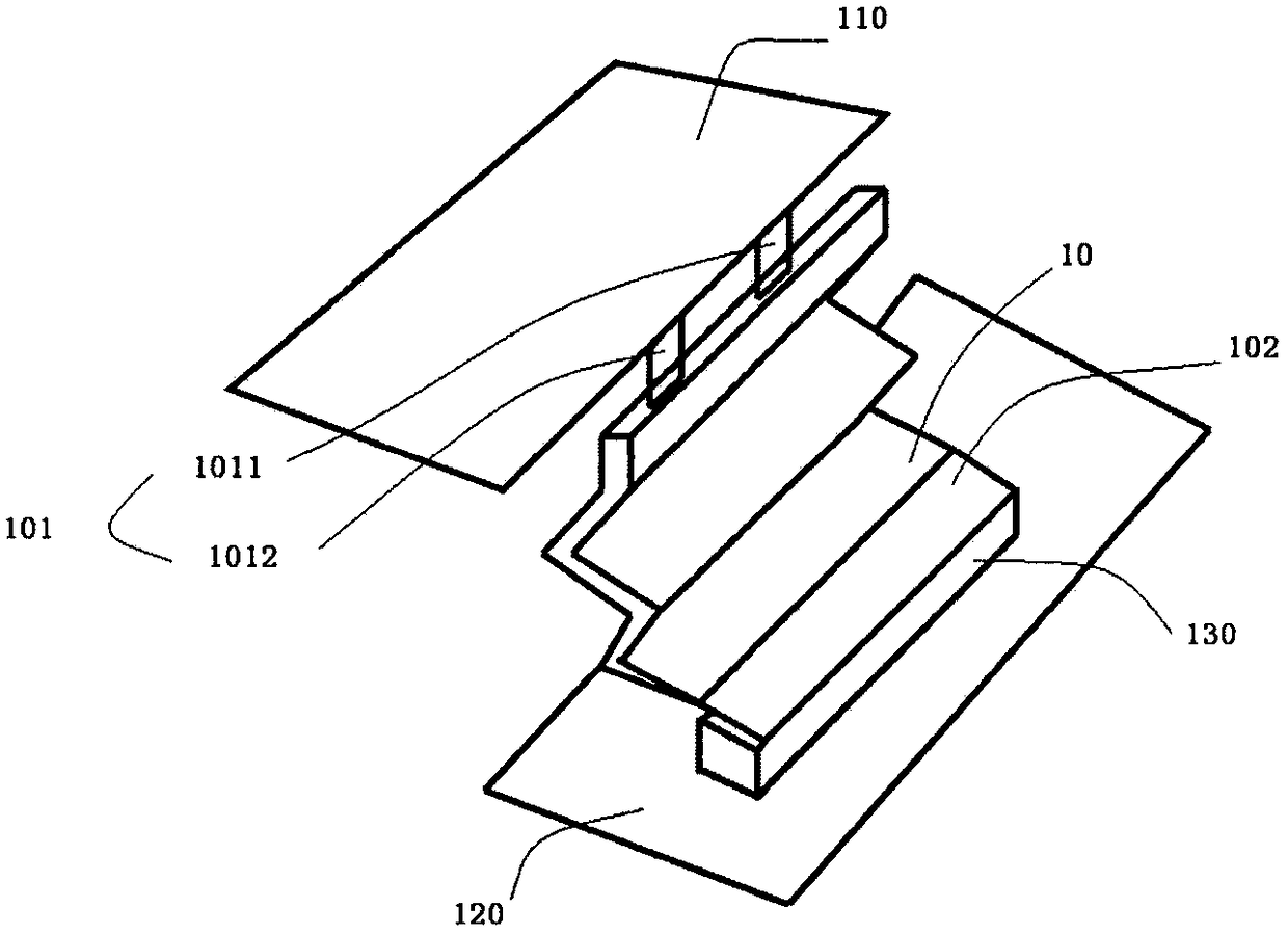
[0031] Please also refer to figure 1 and figure 2 , figure 1 It is a schematic diagram of the three-dimensional structure of the conductive sheet 10 provided by a preferred embodiment of the present invention, figure 2 for application figure 1 Schematic diagram of the connecting device of the middle conductive sheet. In the first embodiment of the present invention, the conductive sheet 10 is according to figure 2 The printed circuit board 110 is shown connected to the ceramic antenna 13 on another printed circuit board 120 . The printed circuit board 110 and the printed circuit board 120 with the ceramic antenna 130 in this embodiment may be two-layer printed circuit boards in any wireless transmission module with a closed metal cavity.

[0032] The conductive sheet 10 includes a first end 101 and a second end 102. In this embodiment, the elastic mode is selected as figure 1 The fold shown. The first end includes two welding parts 1011 and 1012, and the two welding ...

no. 2 example

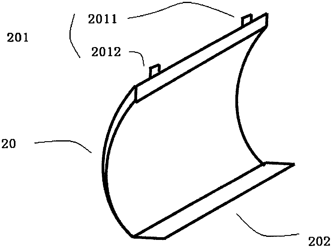
[0034] Please also refer to image 3 , Figure 4 and Figure 5 , image 3 It is a schematic diagram of the three-dimensional structure of the conductive sheet 20 provided by another preferred embodiment of the present invention, Figure 4 for application image 3 Schematic diagram of the connection device of the conductive sheet in the middle, Figure 5 It is a perspective view of a wireless transmitting module containing a ceramic antenna in a closed metal cavity applying the present invention. According to the first embodiment of the present invention, the conductive sheet 20 is Figure 4 The printed circuit board 210 is shown connected to the ceramic antenna 13 on another printed circuit board 220 . The connecting device 260 of the present invention presses Figure 5 Mounted within metal cavity 250 as shown. The printed circuit board 210 and the printed circuit board 220 with the ceramic antenna 230 in this embodiment may be two-layer printed circuit boards in any w...


PUM


Abstract

The invention provides a connection device of a ceramic antenna and a printed circuit board. The connection device is composed of a ceramic antenna, a conducting plate and a printed circuit board. Theceramic antenna is fixed at the printed circuit board. The conducting plate has a first end and a second end and is connected to the ceramic antenna and the printed circuit board elastically. The first end of the conducting plate is fixed at the printed circuit board by welding and is connected to other signal transmitting devices electrically and the second end is in contact above the ceramic antenna. According to the connection device, a shielded signal of the ceramic antenna can be transmitted out of a closed metal cavity by the conducting plate, so that a signal shielding problem caused by the closed metal cavity is solved.

Description

technical field [0001] The invention relates to a connection device between a ceramic antenna and a printed circuit board, in particular to a wireless transmitting module applied to a closed metal cavity containing a ceramic antenna. Background technique [0002] Antennas are common signal communication components and are often applied to wireless communication devices. With the vigorous development of wireless communication, in order to meet this demand, some embedded antennas are also required to be small in size, thus giving birth to the emergence of ceramic antennas. Following this trend, many electronic products have applied ceramic antennas. Due to aesthetic requirements, many electronic products need to be equipped with metal casings. However, the metal casing will cause interference to the antenna built in the casing, so that the signal cannot be transmitted through the metal casing. Therefore, how to transmit the shielded signal on the ceramic antenna from the in...

Claims


Application Information

Patent Timeline
Patent Type & Authority Applications(China)
IPC IPC(8): H01R11/01H01R11/05H01R12/55H01R4/48H01Q1/22
CPCH01R11/01H01Q1/22H01R4/4809H01R11/05H01R12/55
Inventor 张成张晨
Owner 南京舒尔斯科技有限公司
Why Eureka
Try Eureka