
Gallium nitride crystal manufacturing method and substrate

A manufacturing method and gallium nitride technology, applied in chemical instruments and methods, crystal growth, from chemically reactive gases, etc., can solve problems such as unobtainable and unstable semi-polar GaN crystal planes

Inactive Publication Date: 2018-08-10
XIAN SAIFULESI SEMICON TECH CO LTD
View PDF7 Cites 3 Cited by
  • Summary
  • Abstract
  • Description
  • Claims
  • Application Information

AI Technical Summary

Problems solved by technology

[0005] Therefore, using hydrogen as a carrier gas cannot obtain those energetically unstable semi-polar GaN crystal planes.

Method used

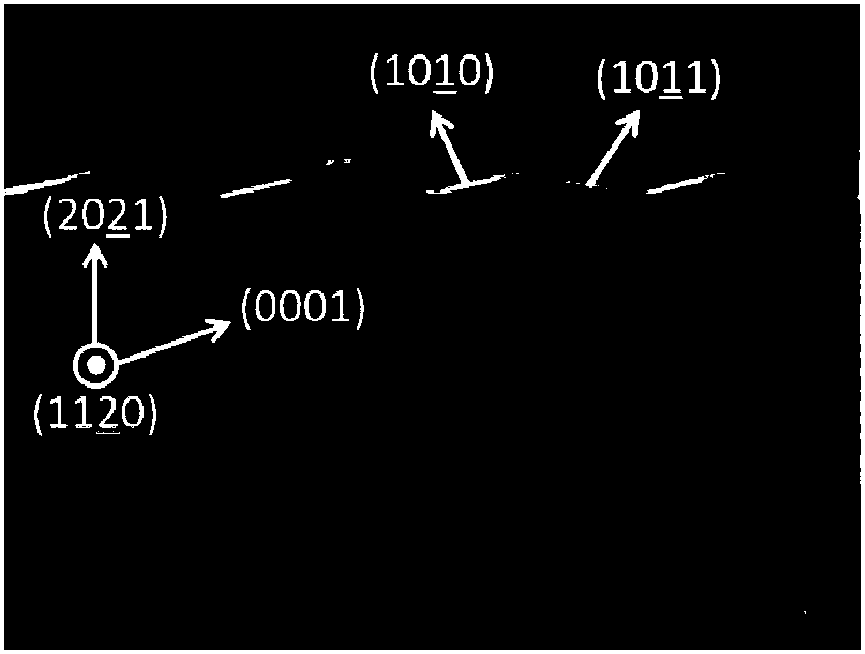
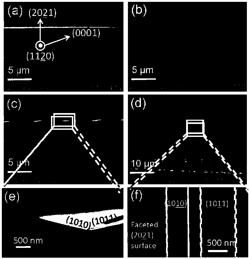
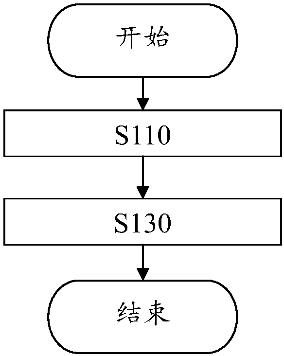

Image

  • Gallium nitride crystal manufacturing method and substrate
  • Gallium nitride crystal manufacturing method and substrate
  • Gallium nitride crystal manufacturing method and substrate

Examples


Embodiment Construction

[0031] Reference will now be made in detail to the exemplary embodiments, examples of which are illustrated in the accompanying drawings. When the following description refers to the accompanying drawings, the same numerals in different drawings refer to the same or similar elements unless otherwise indicated. The implementations described in the following exemplary examples do not represent all implementations consistent with the present disclosure. Rather, they are merely examples of apparatuses and methods consistent with aspects of the present disclosure as recited in the appended claims.

[0032] The terminology used in the present disclosure is for the purpose of describing particular embodiments only and is not intended to limit the present disclosure. Unless otherwise defined, all other scientific and technical terms used herein have the same meaning as commonly understood by one of ordinary skill in the art to which this invention belongs. As used in this disclosure...


PUM

PropertyMeasurementUnit
thicknessaaaaaaaaaa
thicknessaaaaaaaaaa
thicknessaaaaaaaaaa

Abstract

The invention relates to a gallium nitride crystal manufacturing method and a substrate. The method comprises the following steps: carrying out first epitaxial growth under in a first atmosphere to form a first gallium nitride crystal layer on a patterned surface of a sapphire substrate; and carrying out second epitaxial growth in a second atmosphere different from the first atmosphere to form a second gallium nitride crystal layer on the surface of the first gallium nitride crystal layer. With the manufacturing method, the gallium nitride crystal with a smooth semi-polar crystal face can be obtained with a mode of not using chemical mechanical polishing.

Description

technical field [0001] The present disclosure relates to a gallium nitride crystal manufacturing method and substrate Background technique [0002] In recent years, some Gallium Nitride (GaN) research institutions and companies such as the University of California at Santa Barbara in the United States and SONY and SUMITOMO in Japan have successfully prepared high-power, High-efficiency blue and green light-emitting diodes and laser diodes, etc. These special crystal planes of GaN (such as (20 2 1), (30 3 1) has great potential and advantages in high-efficiency, low-efficiency-droop light-emitting diodes (LEDs) and high-power long-wavelength laser diodes (LDs). [0003] When preparing some semipolar GaN crystal thin film materials with special crystal orientations, because the GaN crystal planes of these semipolar crystal orientations are energy unstable planes, such as (20 2 1), (30 3 1), (20 2 1) and (30 3 1), etc., but the epitaxial growth process of GaN used to man...

Claims


Application Information

Patent Timeline
Patent Type & Authority Applications(China)
IPC IPC(8): C30B25/14C30B25/18C30B29/40
CPCC30B25/14C30B25/186C30B29/406
Inventor 陈辰宋杰崔周源
Owner XIAN SAIFULESI SEMICON TECH CO LTD
Learn More