Single step pendeo-and lateral epitaxial overgrowth of group III-nitride epitaxial layers with group III-nitride buffer layer and resulting structures

Inactive Publication Date: 2002-02-21
CREE INC
View PDF0 Cites 176 Cited by
  • Summary
  • Abstract
  • Description
  • Claims
  • Application Information

AI Technical Summary

Benefits of technology

0007] Accordingly, there is a need in the art for a method of fabricating a relatively defect-free single cry

Problems solved by technology

High-quality bulk crystals of GaN are currently unavailable for commercial use. tThus, GaN crystals are typically fabricated as heteroepitaxial layers on underlying non-GaN substrates.
Unfortunately, GaN has a considerable lattice mismatch with most suitable substrate crystals.
Such def

Method used


Image

  • Single step pendeo-and lateral epitaxial overgrowth of group III-nitride epitaxial layers with group III-nitride buffer layer and resulting structures
  • Single step pendeo-and lateral epitaxial overgrowth of group III-nitride epitaxial layers with group III-nitride buffer layer and resulting structures
  • Single step pendeo-and lateral epitaxial overgrowth of group III-nitride epitaxial layers with group III-nitride buffer layer and resulting structures

Examples


example 2

[0077] EXAMPLE 2

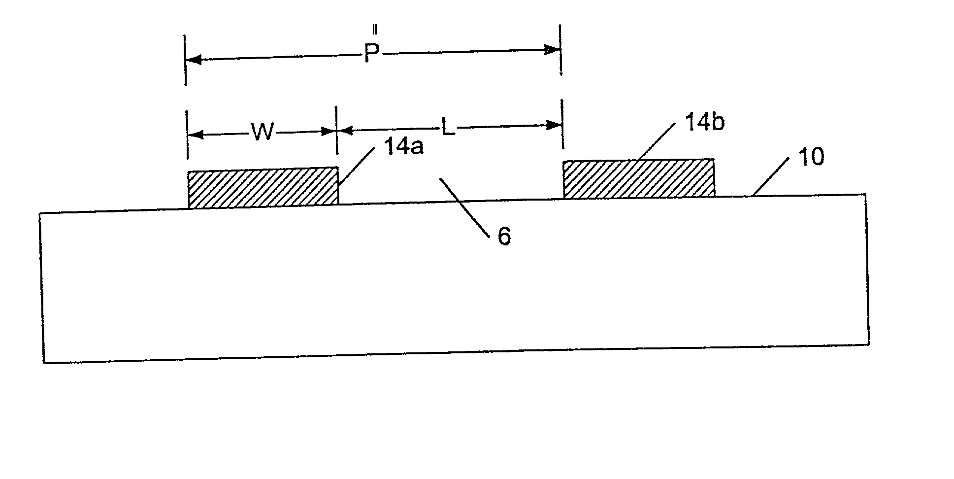
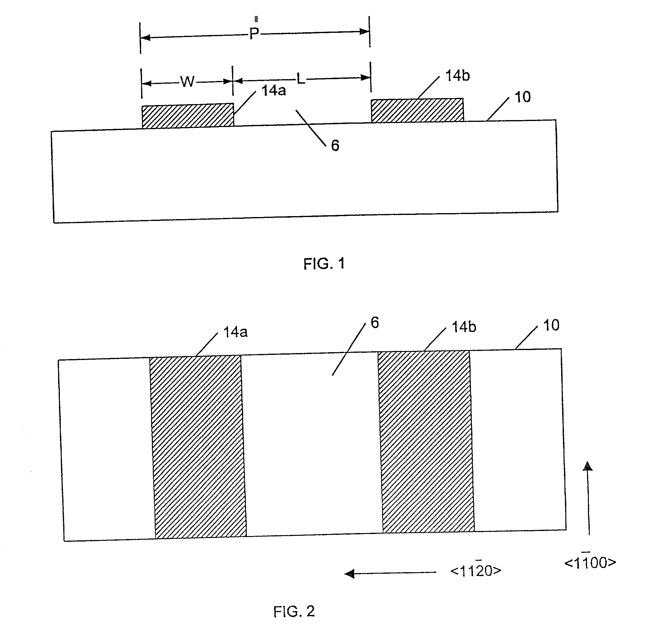
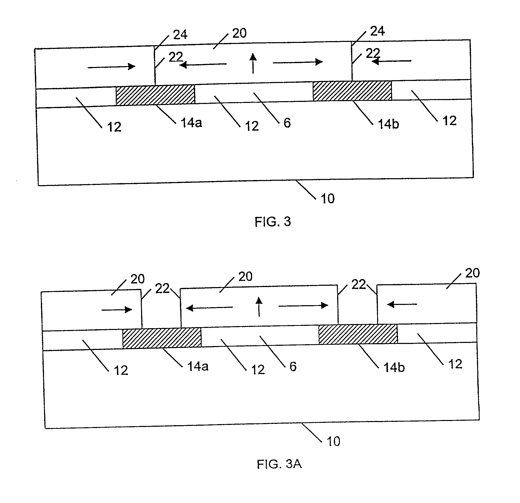
[0078] A patterned mask of Si.sub.xN.sub.y stripes having a stripe width of 10.mu., a window length of 25.mu. and a period of 35.mu. for a fill factor of 0.715 was applied to a 6H--SiC substrate. The stripes were arranged parallel to the direction. A 0.5.mu. thick Al.sub.0.1Ga.sub.0.9N buffer layer was grown by MOVPE by flowing TMG at 34.8 .mu.mol / min, TMA at 6.51 .mu.mol / min and ammonia at 10 slpm in a diluent of H.sub.2 at 15.5 slpm at 1050.degree. C. and 76 Torr for a total of 80 minutes. Following growth of the buffer layer, an epitaxial layer of GaN was grown by MOVPE by flowing TMG at 309 .mu.mol / min and ammonia at 17 slpm in a diluent of H.sub.2 at 22.5 slpm at 1060.degree. C. and 200 Torr for one hour. The ratio of lateral to vertical growth under these conditions was approximately 1:1. FIG. 16 is an SEM image a cross section of the resulting GaN layer.


PUM


Abstract

A method of fabricating a gallium nitride-based semiconductor structure on a substrate includes the steps of forming a mask having at least one opening therein directly on the substrate, growing a buffer layer through the opening, and growing a layer of gallium nitride upwardly from the buffer layer and laterally across the mask. During growth of the gallium nitride from the mask, the vertical and horizontal growth rates of the gallium nitride layer are maintained at rates sufficient to prevent polycrystalline material nucleating on said mask from interrupting the lateral growth of the gallium nitride layer. In an alternative embodiment, the method includes forming at least one raised portion defining adjacent trenches in the substrate and forming a mask on the substrate, the mask having at least one opening over the upper surface of the raised portion. A buffer layer may be grown from the upper surface of the raised portion. The gallium nitride layer is then grown laterally by pendeoepitaxy over the trenches.

Description

[0001] The present invention relates to electronic device structures and fabrication methods, and more particularly to Group III-nitride semiconductor structures and methods of fabrication by pendeo- and lateral epitaxial overgrowth.[0002] Gallium nitride (GaN) is a wide-bandgap semiconductor material widely known for its usefulness as an active layer in blue light emitting diodes. GaN is also under investigation for use in other microelectronic devices including laser diodes and high-speed, high power transistor devices. As used herein, "gallium nitride" or "GaN" refers to gallium nitride and III-nitride alloys thereof, including aluminum gallium nitride (AlGaN), indium gallium nitride (InGaN) and aluminum indium gallium nitride (AlInGaN).[0003] High-quality bulk crystals of GaN are currently unavailable for commercial use. tThus, GaN crystals are typically fabricated as heteroepitaxial layers on underlying non-GaN substrates. Unfortunately, GaN has a considerable lattice mismatch ...

Claims


Application Information

Patent Timeline
IPC IPC(8): H01L21/20H01L21/205H01S5/02
CPCH01L21/0237H01L21/02378H01L21/02458H01L21/02491H01L21/0254H01L21/0262H01L21/02639H01L21/02642H01L21/02647H01L21/0265H01S5/3202H01S2304/12H01S5/320225
Inventor KONG, HUA-SHUANGEDMOND, JOHN ADAMHABERERN, KEVIN WARDEMERSON, DAVID TODD
Owner CREE INC
Why Eureka
Try Eureka