
Eureka
For R&D, Eureka makes reading and utilizing patents & technical documents easy.
Eureka AIR
Designed for self-driven R&D workflows. Generate viable solutions, solve complex R&D challenges, empower your innovation with AI.

Eureka Materials
Designed for material experts only. Revolutionize your material R&D, from search, analyze, to developing new materials.

TechResearch
Generate reliable direction feasibility study reports for your R&D in just a few steps.

TechSeek
Discover and master advanced knowledge NOW. Basics, ideas, possibilities, all at once.

TechMind
As an expert in R&D Theories, TechMind can generates customized viable solutions instantly.

TechRisk
Analyze your overall solution with one click, know your potential R&D risks in advance.

TechMonitor
Get weekly tech updates, stay abreast of the latest tech innovations and key insights.
Semiconductor optical module and carrier
A semiconductor and optical module technology, applied in the direction of semiconductor lasers, semiconductor devices, semiconductor/solid-state device components, etc., can solve problems such as changes in the characteristics of semiconductor optical devices, and achieve the effect of suppressing changes in characteristics
- Summary
- Abstract
- Description
- Claims
- Application Information
AI Technical Summary
Problems solved by technology
Method used
Image

Examples
Embodiment Construction
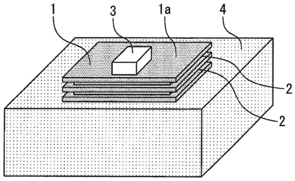
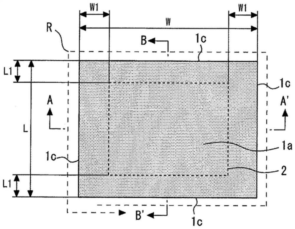
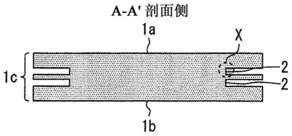
[0055] figure 1 It is a perspective view showing the state in which the semiconductor chip 3 is mounted on the carrier 1 which concerns on embodiment of this invention. figure 2 It is a plan view of the carrier 1 according to the embodiment of the present invention, image 3 is vector 1 along the figure 2 A cross-sectional view of line A-A' in, Figure 4 is vector 1 along the figure 2 The cross-sectional view of the line B-B' in.
[0056] exist figure 1 The middle figure shows the stacked structure of the carrier 4 , the carrier 1 and the semiconductor chip 3 . use Image 6 , Figure 7 , Figure 9 and Figure 10 The semiconductor optical modules 10, 110, and 210 described later have the same figure 1 Same stack structure. Alternatively, just use Figure 8 For the semiconductor optical module 50 described later, the support body 4 is not provided, and the carrier 1 is directly fixed to the stem 20 (refer to Figure 8 ). As described above, the carrier 1 is inco...
PUM
 Abstract
Description
Claims
Application Information
 - R&D Engineer
- R&D Manager
- IP Professional
- Industry Leading Data Capabilities
- Powerful AI technology
- Patent DNA Extraction
Browse by: Latest US Patents, China's latest patents, Technical Efficacy Thesaurus, Application Domain, Technology Topic, Popular Technical Reports.
© 2024 PatSnap. All rights reserved.Legal|Privacy policy|Modern Slavery Act Transparency Statement|Sitemap|About US| Contact US: help@patsnap.com