
Optical scanning device and optical scanning method

A technology of optical scanning device and mirror, applied in optics, optical components, instruments, etc., can solve the problems of difficult compensation accuracy, regardless of vertical beam phase shift, etc., and achieve the effect of improving compensation accuracy

Active Publication Date: 2021-11-09
MITSUMI ELECTRIC CO LTD
View PDF11 Cites 0 Cited by
  • Summary
  • Abstract
  • Description
  • Claims
  • Application Information

AI Technical Summary

Problems solved by technology

[0005] However, in the prior art disclosed in Patent Document 1, it is difficult to improve the compensation accuracy of the phase shift in the horizontal scanning direction without considering the phase shift caused by the bending change of the vertical beam.

Method used


Image

  • Optical scanning device and optical scanning method
  • Optical scanning device and optical scanning method
  • Optical scanning device and optical scanning method

Examples


no. 1 approach

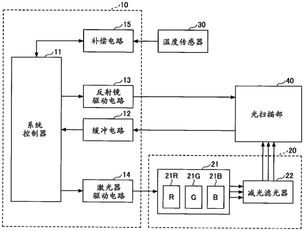
[0025] Hereinafter, a first embodiment will be described with reference to the drawings. figure 1 The structure of the optical scanning device of the first embodiment will be described.

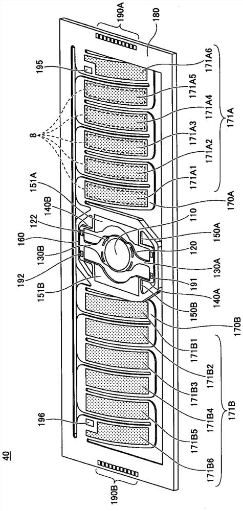
[0026] The optical scanning device 1 of the present embodiment includes an optical scanning control unit 10 , a light source unit 20 , a temperature sensor 30 , and an optical scanning unit 40 . Each part will be described below.

[0027] The light scanning control unit 10 of the present embodiment controls the light source unit 20 and the light scanning unit 40 . The optical scanning control unit 10 includes a system controller 11 , a buffer circuit 12 , a mirror drive circuit 13 , a laser drive circuit 14 , and a compensation circuit 15 .

[0028] The system controller 11 supplies the mirror driving circuit 13 with a control signal for controlling the oscillation of the mirror included in the optical scanning unit 40 . In addition, the system controller 11 supplies a digital video signal...

no. 2 approach

[0103] Hereinafter, a second embodiment will be described. The second embodiment differs from the first embodiment in that it is determined whether the bending state of the driving beam that oscillates the mirror in the vertical direction is stable, and if it is stable, the phase shift is not compensated using the difference in bending. In the following description of the second embodiment, only the differences from the first embodiment will be described, and the components having the same functional structure as those of the first embodiment will be given the same symbols as those used in the description of the first embodiment, and Its description is omitted.

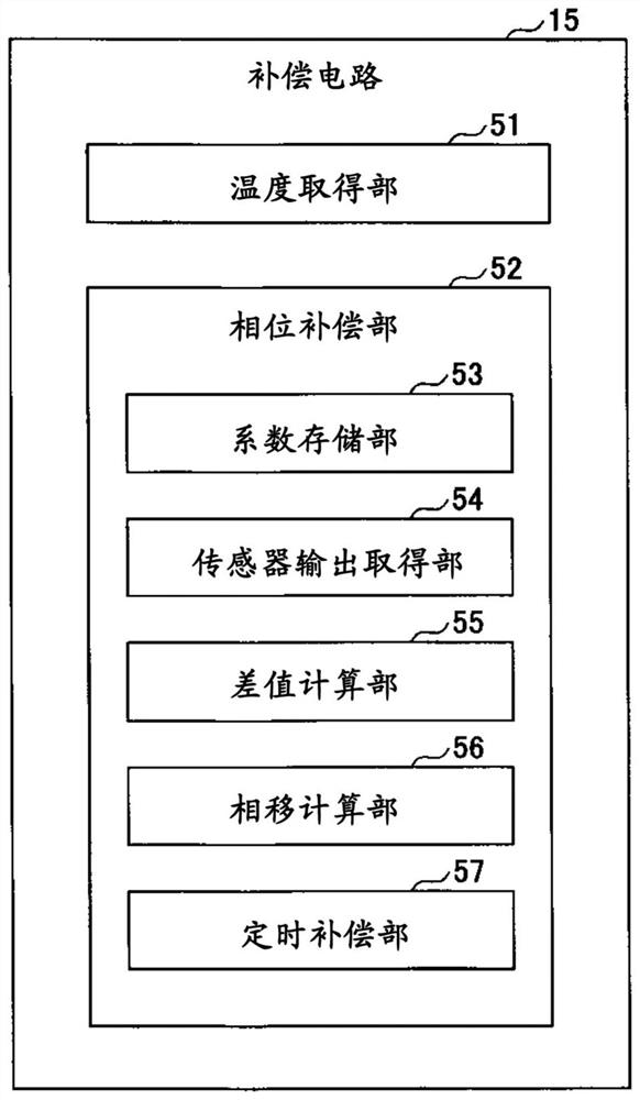
[0104] Figure 7 It is a figure explaining the function of the compensation circuit of 2nd Embodiment. The compensation circuit 15A of the present embodiment includes a temperature acquisition unit 51 and a phase compensation unit 52A.

[0105] The phase compensator 52A of the present embodiment includes a coeffici...


PUM


Abstract

The present invention relates to an optical scanning device and an optical scanning method. The purpose is to improve the compensation accuracy of the phase shift in the horizontal scanning direction. A two-dimensional scanning optical scanning device that oscillates a mirror in a first direction and a second direction that is perpendicular to the first direction includes: a difference calculation unit that calculates a second value for oscillating the mirror in the second direction. The difference between the amount of bending when the second driving beam is initially driven and the amount of bending when the second driving beam is driven for a predetermined time; The amount of phase shift between the driving signal for shaking in the first direction and the signal representing the displacement of the mirror in the first direction.

Description

technical field [0001] The present invention relates to an optical scanning device and an optical scanning method. Background technique [0002] Currently known is a light scanning device that drives a MEMS (Micro Electro Mechanical System) mirror (Mirror) to sequentially change the reflection direction of laser light, thereby scanning the laser light two-dimensionally and projecting an image. [0003] In addition, it is conventionally known that in the horizontal driving of the MEMS mirror, when relatively high-speed resonance driving is used, a phase difference occurs between the driving signal and the displacement of the MEMS mirror. When this phase difference occurs, a shift corresponding to the phase difference in the horizontal scanning direction occurs in the projected image. Therefore, a technique capable of canceling such a phase shift in the horizontal scanning direction is currently required (Patent Document 1). [0004] It is known that even at a constant tempe...

Claims


Application Information

Patent Timeline
Patent Type & Authority Patents(China)
IPC IPC(8): G02B26/10G02B26/08G09G3/02G09G3/34
CPCG02B26/0858G02B26/101G09G3/025G09G3/346G02B26/10
Inventor 木村佑司
Owner MITSUMI ELECTRIC CO LTD
Learn More