Optical film material structure and formation method thereof, and display device

A technology of optical film materials and display devices, applied in optics, optical components, nonlinear optics, etc., can solve problems such as decreased picture definition and lowered display quality, and achieves elimination of regular distribution, cost reduction, and resolution reduction required effect

Active Publication Date: 2018-08-24
BOE TECH GRP CO LTD +1
View PDF8 Cites 6 Cited by
  • Summary
  • Abstract
  • Description
  • Claims
  • Application Information

AI Technical Summary

Problems solved by technology

[0002] At present, virtual / augmented reality display devices usually have a larger display viewing angle in order to pursue immersion. Therefore, when the display screen is magnified by a lens, its pixels will be magnified several times, making it easy for the human eye to see the display details of a single pixel. , resulting in a decrease in picture clarity, that is, the currently used display screens generally can only meet the requirements of human eyes for picture clarity when viewing directly
The main reason for the above problems is that the black matrix designed to cover the irregular driving lines on the display screen is relatively wide. After being enlarged by the VR imaging lens, the width of the black matrix reaches the limit of human visual resolution, so that the human eye can feel The space matrix effect formed by the black matrix reduces the display quality. This phenomenon is called the screen window effect

Method used


Image

  • Optical film material structure and formation method thereof, and display device
  • Optical film material structure and formation method thereof, and display device
  • Optical film material structure and formation method thereof, and display device

Examples


Embodiment Construction

[0050] Example embodiments will now be described more fully with reference to the accompanying drawings. Example embodiments may, however, be embodied in many forms and should not be construed as limited to the embodiments set forth herein; rather, these embodiments are provided so that this disclosure will be thorough and complete, and will fully convey the concept of example embodiments to those skilled in the art. The same reference numerals in the drawings denote the same or similar structures, and thus their detailed descriptions will be omitted.

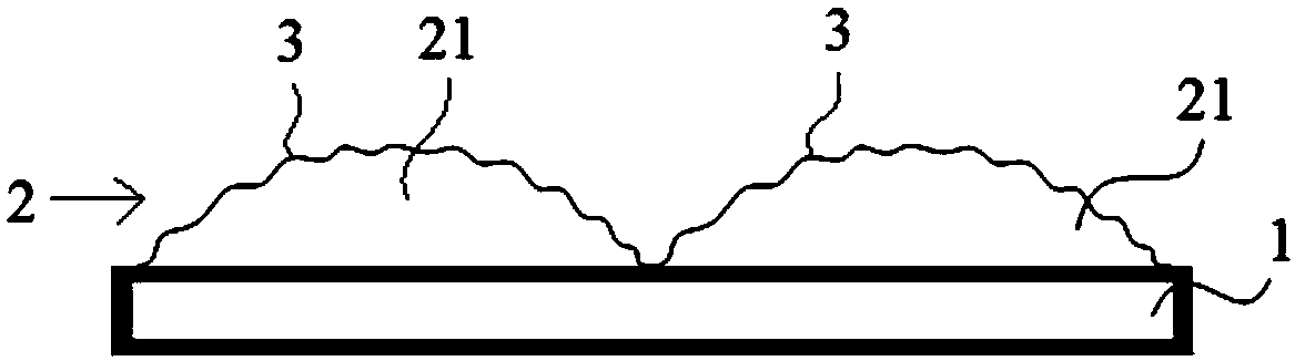
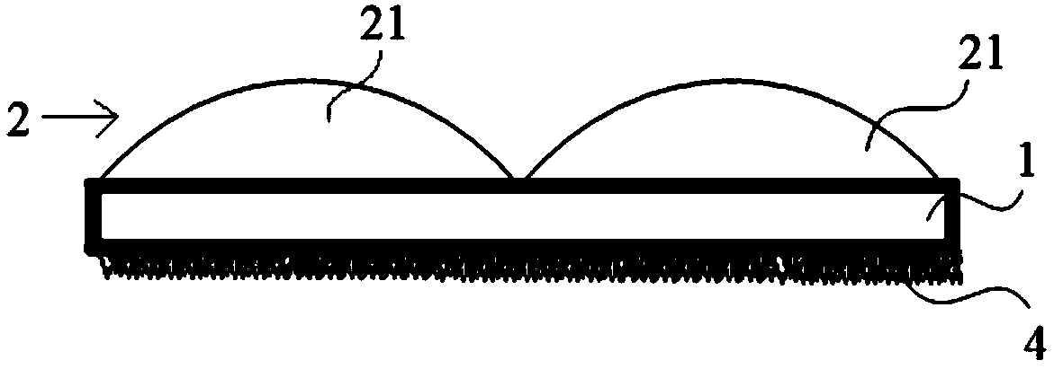
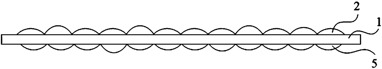
[0051] The present invention firstly provides an optical film structure, which can be used for virtual / augmented reality display screens, and of course can also be used for ordinary display screens, such as computer display screens, TV display screens, and the like. refer to figure 1 Shown is a schematic structural view of an embodiment of the optical film structure of the present invention, the optical film structure may inc...


PUM


Abstract

The present invention relates to the technology field of display, and provides a display device. The display device comprises a display screen, and an optical film material structure arranged at a light-emitting side of the display screen; the optical film material structure comprises a base material layer and a first microlens array layer, and the base material layer has a first surface and a second surface which are oppositely designed; the first microlens array layer is arranged at the at least one o the first surface and the second surface, the first microlens array layer comprises a plurality of microlenses arranged in order, the sizes of the microlenses are smaller than the sizes of subpixels, and seamed edges of adjacent microlenses are mutually overlapped. The display device can improve the screen window effect.

Description

technical field [0001] The invention relates to the field of display technology, in particular to an optical film structure, a method for forming the optical film structure, and a display device equipped with the optical film structure. Background technique [0002] At present, virtual / augmented reality display devices usually have a larger display viewing angle in order to pursue immersion. Therefore, when the display screen is magnified by a lens, its pixels will be magnified several times, making it easy for the human eye to see the display details of a single pixel. , resulting in a decrease in picture definition, that is, the currently used display screens generally can only meet the requirements of human eyes for picture clarity when viewing directly. The main reason for the above problems is that the black matrix designed to cover the irregular driving lines on the display screen is relatively wide. After being enlarged by the VR imaging lens, the width of the black m...

Claims


Application Information

Patent Timeline
Patent Type & Authority Applications(China)
IPC IPC(8): G02B3/00G02F1/1335
CPCG02B3/0006G02F1/133526G02B5/021G02B5/0278G02B5/0294G02F1/133502G02F1/133504G02F1/133562G02B5/0221G02F1/133528G02F1/134309G02F1/134345
Inventor 陈寅伟冯绪清罗振兴肖亮王光泉孙海威高斐
Owner BOE TECH GRP CO LTD
Why Eureka
Try Eureka