Power feed mechanism, rotation pedestal device and semiconductor processing device

A feed-in and power technology, which is applied in the field of rotary base devices, semiconductor processing equipment, and power feed-in mechanisms, can solve problems such as ignition risk, and achieve the effect of avoiding ignition risk and high power transmission efficiency.

Active Publication Date: 2018-08-28
BEIJING NAURA MICROELECTRONICS EQUIP CO LTD
View PDF7 Cites 5 Cited by
  • Summary
  • Abstract
  • Description
  • Claims
  • Application Information

AI Technical Summary

Problems solved by technology

[0008] Second, in order to increase the RF power fed into the base support, it is necessary to increase the voltage of the inductance coil. When the voltage rises to a certain threshold, there is a risk of ignition

Method used


Image

  • Power feed mechanism, rotation pedestal device and semiconductor processing device
  • Power feed mechanism, rotation pedestal device and semiconductor processing device
  • Power feed mechanism, rotation pedestal device and semiconductor processing device

Examples


Embodiment Construction

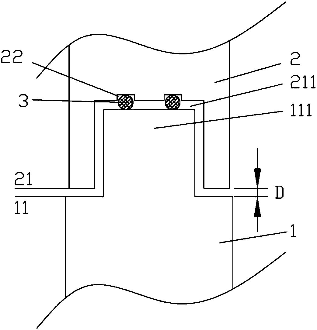
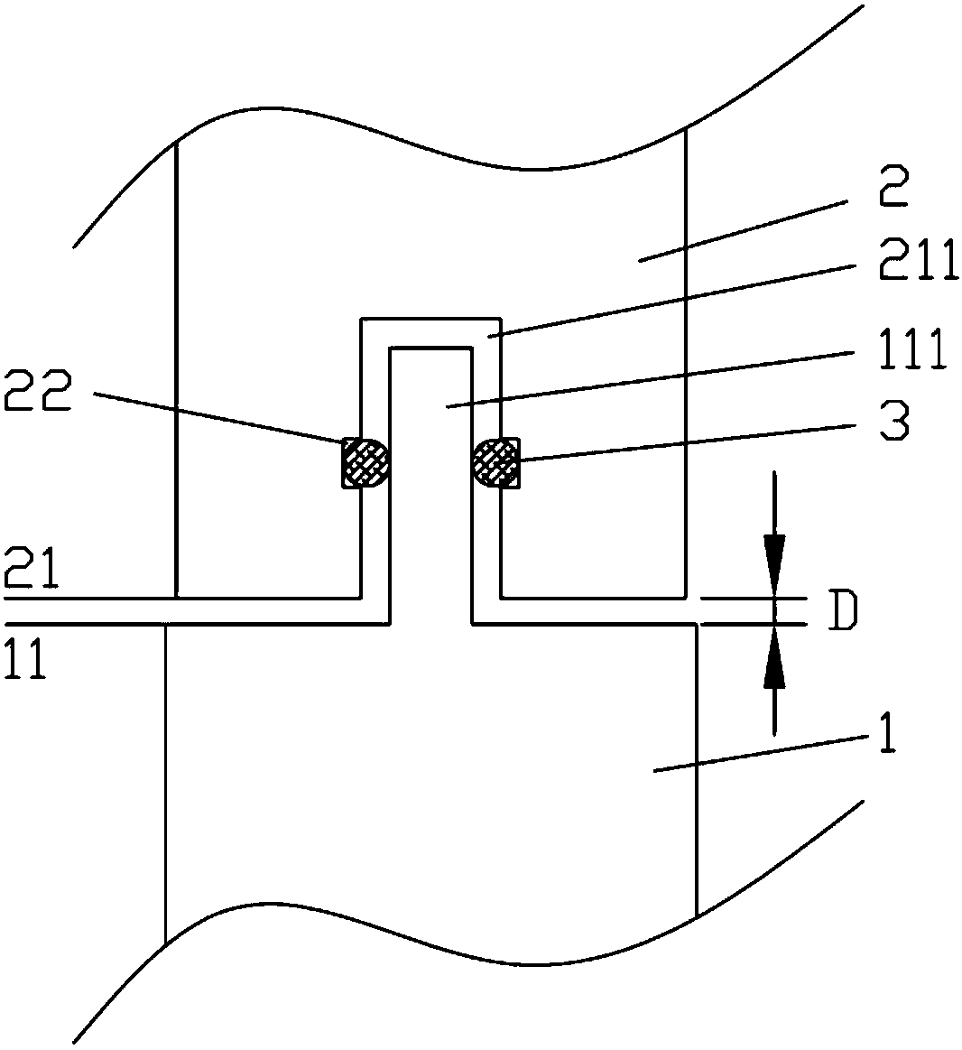
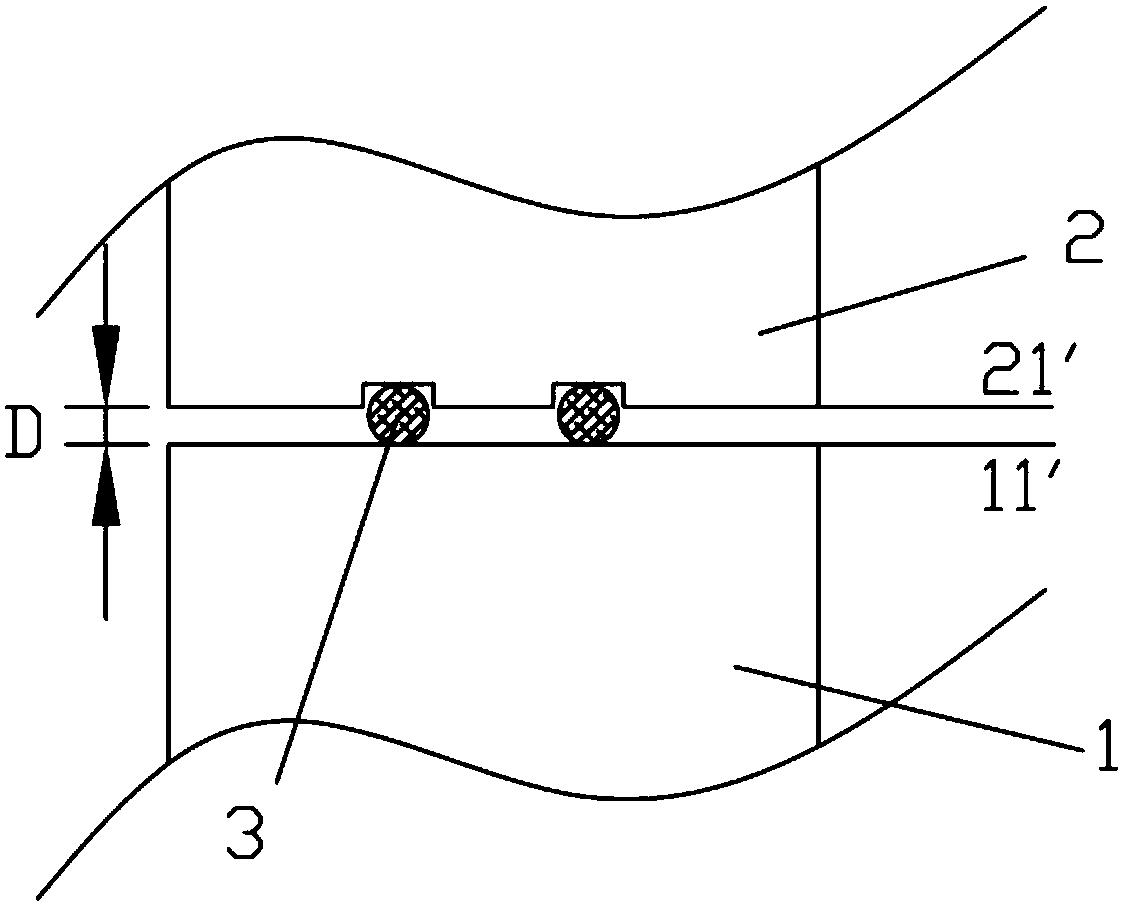
[0054] In order for those skilled in the art to better understand the technical solution of the present invention, the power feeding mechanism, the rotating base device and the semiconductor processing equipment provided by the present invention will be described in detail below with reference to the accompanying drawings.

[0055] The power feed-in mechanism provided by the present invention is used to feed the output power of the power source into the rotatable component. The rotatable component can be a base, a target or a coil, and the like. The power source is usually a matcher and a power supply. The matcher is used to dynamically adjust the variable capacitance in the matching circuit during the process to match the load impedance with the output impedance of the power supply, thereby ensuring the maximum output power of the power supply. applied to the plasma inside the chamber. The power supply includes radio frequency power supply, low frequency power supply, interm...


PUM


Abstract

The present invention provides a power feed mechanism, a rotation pedestal device and a semiconductor processing device. The power feed mechanism is configured to feed an output power of a power source into a rotary part, and comprises: a conductive fixed part electrically connected with the power source; a conductive rotary part electrically connected with the rotary part and configured to perform synchronous rotation with the rotary part; and a conductive connection structure being in electrical contact with the conductive fixed part and the conductive rotary part without influence of rotation motion of the conductive rotary part. The power feed mechanism can improve the power transmission efficiency and can avoid sparking risk in the prior art.

Description

technical field [0001] The invention relates to the technical field of semiconductor manufacturing, in particular to a power feeding mechanism, a rotating base device and semiconductor processing equipment. Background technique [0002] In the PVD (Physical Vapor Deposition, Physical Vapor Deposition) process, the sputtering power supply is introduced into the process chamber through the electrode and then coupled into the process gas to excite the process gas to form a plasma. Under the action of electrons and ions in the plasma, the film is completed deposition. [0003] In the thin film deposition process, there is a high requirement for the uniformity of the deposited thin film, and components such as targets, coils, and bases all have varying degrees of influence on the uniformity. [0004] Films deposited by ordinary PVD processes will have a large residual stress, resulting in a decrease in film quality. For this reason, it is necessary to increase the energy of cha...

Claims


Application Information

Patent Timeline
Patent Type & Authority Applications(China)
IPC IPC(8): H01L21/02H01L21/67H01L21/687
CPCH01L21/02H01L21/67H01L21/68792
Inventor 刘建生李良姜鑫先陈鹏文莉辉
Owner BEIJING NAURA MICROELECTRONICS EQUIP CO LTD
Why Eureka
Try Eureka