
Breakdown electric fuse structure and forming method thereof and semiconductor device

A technology of electric fuses and fuses, which is applied in semiconductor devices, semiconductor/solid-state device manufacturing, semiconductor/solid-state device components, etc., can solve problems such as programming voltage instability, achieve uniform quality, improve performance, and ensure stability Effect

Pending Publication Date: 2018-08-31
CHANGXIN MEMORY TECH INC
View PDF0 Cites 0 Cited by
  • Summary
  • Abstract
  • Description
  • Claims
  • Application Information

AI Technical Summary

Problems solved by technology

[0004] The purpose of the present invention is to provide a breakdown type electric fuse structure to solve the problem that the programming voltage is often unstable in the existing breakdown type electric fuse structure

Method used


Image

  • Breakdown electric fuse structure and forming method thereof and semiconductor device
  • Breakdown electric fuse structure and forming method thereof and semiconductor device
  • Breakdown electric fuse structure and forming method thereof and semiconductor device

Examples


Embodiment 2

[0080] Based on the breakdown electric fuse structure described above, the present invention also provides a method for forming the breakdown electric fuse structure. image 3 It is a schematic flowchart of the method for forming the breakdown electric fuse structure in the second embodiment of the present invention. Such as image 3 As shown, the forming method of the breakdown type electric fuse structure includes:

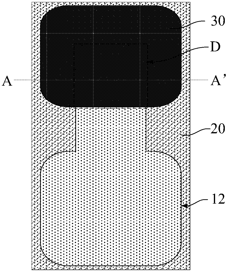
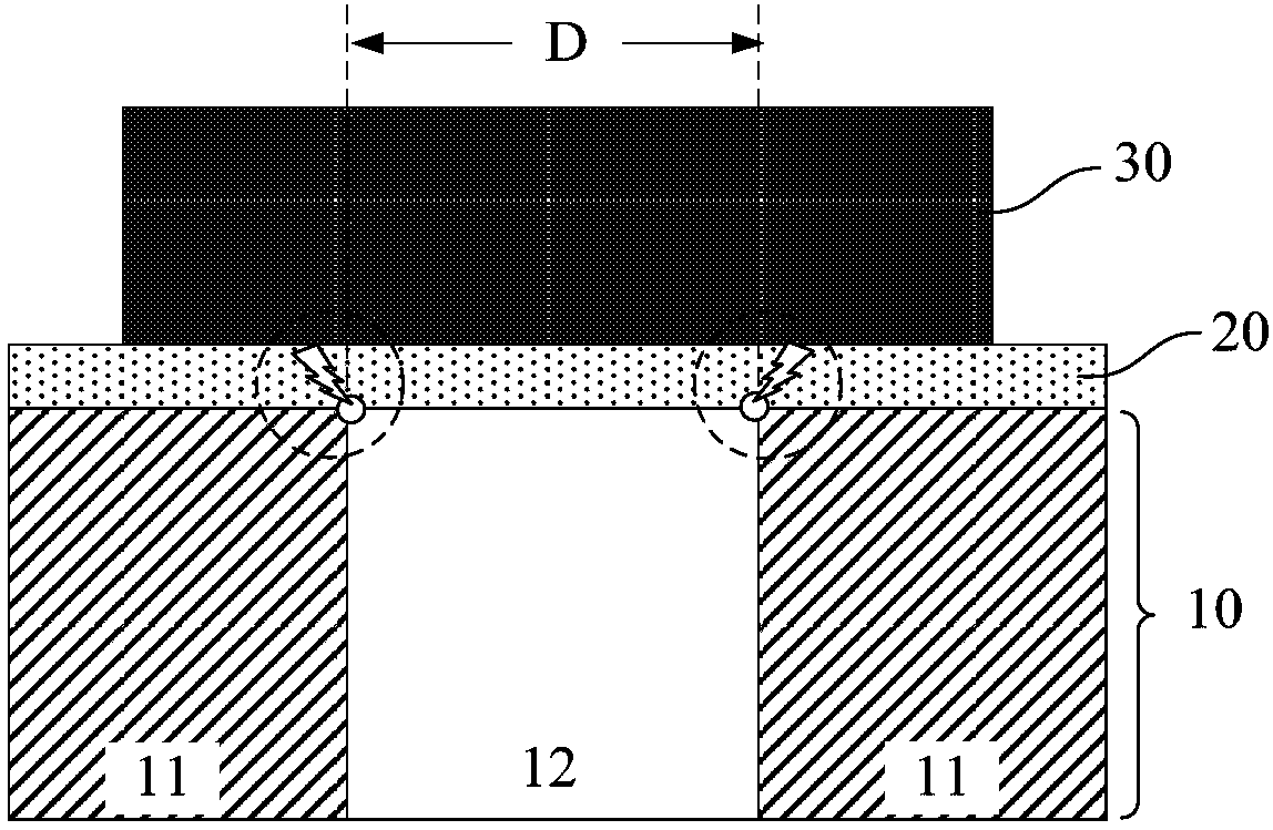
[0081] In step S100 , a substrate is provided, and an isolation structure is formed in the substrate, the isolation structure surrounds an active region in the substrate, and the isolation structure covers a side surface of the active region.

[0082] Step S200, forming an insulating material layer on the substrate, the insulating material layer covers the top surface of the active region and extends to cover the isolation structure around the active region, and in the A breakdown region is defined in the region of the insulating material layer corresponding t...

Embodiment 3

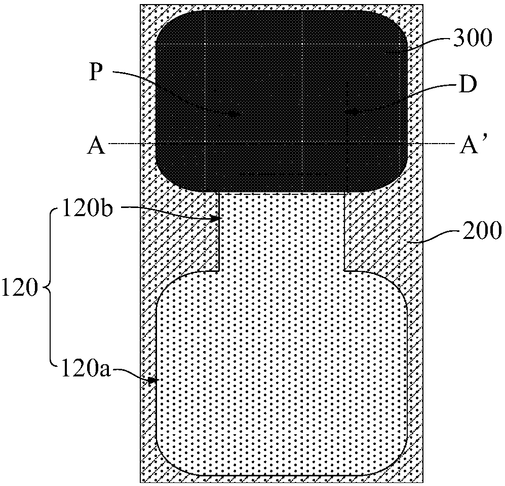
[0105] Based on the breakdown type electric fuse structure as described above, the present invention also provides a semiconductor device including the breakdown type electric fuse structure. For example, the semiconductor device is a memory.

[0106] Wherein, the memory further includes a storage unit. Optionally, the breakdown electric fuse structure may be used to form a part of the storage unit of the memory, so as to realize data storage. Specifically, the memory cell includes, for example, a selection transistor and the breakdown electric fuse structure, and the breakdown electric fuse structure is connected to the selection transistor.

[0107] When programming the selected memory cell, the selection transistor corresponding to the selected memory cell is turned on, and a high voltage is input, and the high voltage is applied to the breakdown type electric fuse structure, so that the breakdown The type electric fuse structure is broken down, and then turns from high r...


PUM

PropertyMeasurementUnit
Thicknessaaaaaaaaaa
Thicknessaaaaaaaaaa

Abstract

The invention provides a breakdown electric fuse structure and a forming method thereof and a semiconductor device. A breakdown region is defined in an insulating material layer, and the boundary of the breakdown region is located in an area range of an active region and is not bordered on the boundary of an isolation structure, so that the possibility of breakdown at the part, corresponding to the boundary of the active region, of the insulating material layer can be removed and the problem that programming voltage is unstable due to a boundary defect of the active region can be solved. Therefore, the stability of the programming voltage of the breakdown electric fuse structure can be improved; and furthermore, the insulating material layer in the breakdown region has unique quality, so that the insulating material layer can be uniformly broken down and a uniform current circulation channel can be correspondingly provided.

Description

technical field [0001] The invention relates to the technical field of semiconductors, in particular to a breakdown electric fuse structure and its forming method, and a semiconductor device. Background technique [0002] Fuse structures are widely used in current integrated circuits to selectively connect or disconnect semiconductor devices from other parts of the circuit and to provide logic operations. The fuse structure generally has two types: a blown fuse structure and a breakdown fuse structure. Among them, after the blown fuse structure is activated, the fuse can be melted, disconnected, etc., to interrupt or disconnect the electrical connection, so that the circuit resistance increases, thereby providing an activated fuse structure and an unactivated blown fuse structure. Logical difference between wire structures. And, the breakdown fuse structure works just the opposite of the blown fuse structure. The breakdown fuse structure is non-conductive when it is not ac...

Claims


Application Information

Patent Timeline
IPC IPC(8): H01L21/02H01L21/768H01L23/532
CPCH01L23/53204H01L21/02H01L21/768
Inventor 不公告发明人
Owner CHANGXIN MEMORY TECH INC
Features
  • Generate Ideas
  • Intellectual Property
  • Life Sciences
  • Materials
  • Tech Scout
  • Unparalleled Data Quality
  • Higher Quality Content
  • 60% Fewer Hallucinations
Learn More