Method for packaging display panel

A display panel and packaging method technology, which is applied in the manufacture of electrical components, electrical solid devices, semiconductor/solid devices, etc., can solve the problems of easy cracks in the cathode layer, and achieve the goals of avoiding cracks, reducing force, and improving yield Effect

Active Publication Date: 2018-08-31
BOE TECH GRP CO LTD
View PDF5 Cites 3 Cited by
  • Summary
  • Abstract
  • Description
  • Claims
  • Application Information

AI Technical Summary

Problems solved by technology

[0005] The present invention aims at the above-mentioned deficiencies in the prior art, and provides a packaging method for a display

Method used


Image

  • Method for packaging display panel
  • Method for packaging display panel
  • Method for packaging display panel

Examples


Example Embodiment

[0034] In order to enable those skilled in the art to better understand the technical solutions of the present invention, a method for packaging a display panel provided by the present invention will be described in detail below with reference to the accompanying drawings.
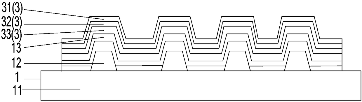
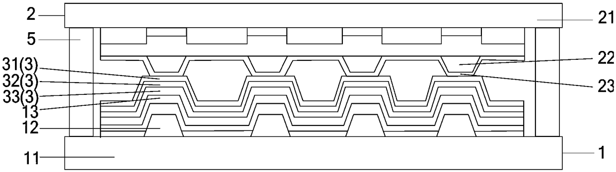
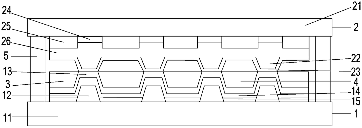
[0035] The embodiment of the present invention provides a packaging method of a display panel, such as image 3 As shown, the display panel may include a first substrate 1 and a second substrate 2. The first substrate 1 may include a first base 11, a pixel defining layer 12 formed on the first base 11, and a pixel defining layer 12 formed on the The first electrode layer 13, the pixel defining layer 12 may define a plurality of pixel units 4 on the first substrate 11; the second substrate 2 may include a second substrate 21, spacers 22 formed on the second substrate 21, and The second electrode layer 23 formed on the spacer 22 can keep the cell thickness of each position of the display panel uniform.

[0036] S...


PUM

PropertyMeasurementUnit
Melting pointaaaaaaaaaa

Abstract

The invention provides a method for packaging a display panel. The method comprises: at least two stacked solid-state packaging layers are formed at one side, away from a first substrate, of a first electrode layer, wherein the melting points of the packaging layers are different; the first substrate and a second substrate are paired, so that a spaced pad corresponds to a pixel defining layer; andthen all packaging layers are heated and pressures are applied to the first substrate and/or the second substrate, so that the first electrode layer and the second electrode layer are in contact. During the packaging process of the display panel, all packaging layers are transformed from solid states to liquid states successively and all corresponding packaging layers are compressed one by one; and during the compression processes of all packaging layers, the stresses generated inside the packaging layers are small because of the small deformation quantities of all packaging layers, so that the acting force on the first electrode layer by the whole packaging layer is reduced and thus the cracks at the first electrode layer are avoided. Therefore, the yield of the OLED display panel is improved.

Description

technical field [0001] The invention relates to the field of display technology, in particular to a packaging method for a display panel. Background technique [0002] Due to the advantages of OLED (Organic Light-Emitting Diode, organic light-emitting diode) display panel with all-solid structure, high brightness, full viewing angle, fast response speed and flexible display, it has become a very competitive and promising next-generation display product . The existing OLED display panel includes a first substrate and a second substrate. The first substrate includes a first substrate and a pixel definition layer, an anode layer, an organic light-emitting layer, and a cathode layer sequentially formed on the first substrate. The second substrate includes a second substrate. The base and the black matrix, the color filter layer, the planarization layer and the spacer are sequentially formed on the second substrate. [0003] Since the thickness of the cathode layer is relativel...

Claims


Application Information

Patent Timeline
IPC IPC(8): H01L51/56
CPCH10K71/50H10K71/00
Inventor 宋文峰
Owner BOE TECH GRP CO LTD
Why Eureka
Try Eureka