Driving circuit of organic light emitting display

A technology of light-emitting display and drive circuit, which is applied to static indicators, instruments, etc., can solve problems affecting the display brightness of organic light-emitting diodes (OLEDs), achieve the effect of improving accuracy and realizing narrow borders

Active Publication Date: 2018-09-04
NANJING CEC PANDA LCD TECH
View PDF7 Cites 2 Cited by
  • Summary
  • Abstract
  • Description
  • Claims
  • Application Information

AI Technical Summary

Problems solved by technology

When the switching transistor T1 is turned off, the parasitic capacitance Cgd between the gate and the drain of the switching transistor T1 will cause the voltage level of the data node NetA (that is, the gate voltage value of the driving transistor T2) to be affected and change the jump voltage (Feed through voltage) △Vp, the gate voltage of the driving transistor T2 becomes Vdate-|△Vp|, which affects the display brightness of the organic light-emitting diode OLED

Method used


Image

  • Driving circuit of organic light emitting display
  • Driving circuit of organic light emitting display
  • Driving circuit of organic light emitting display

Examples


Embodiment 1

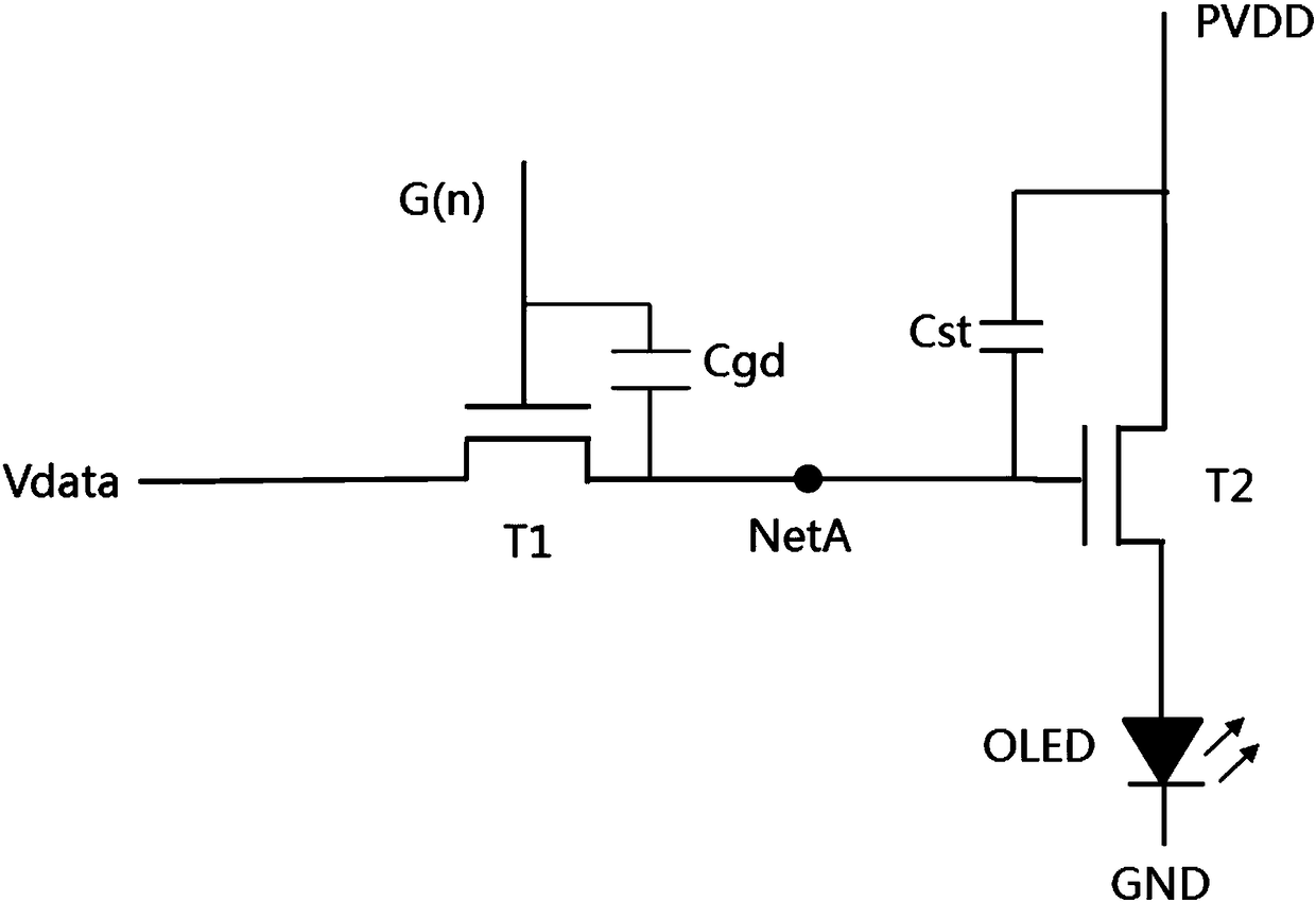
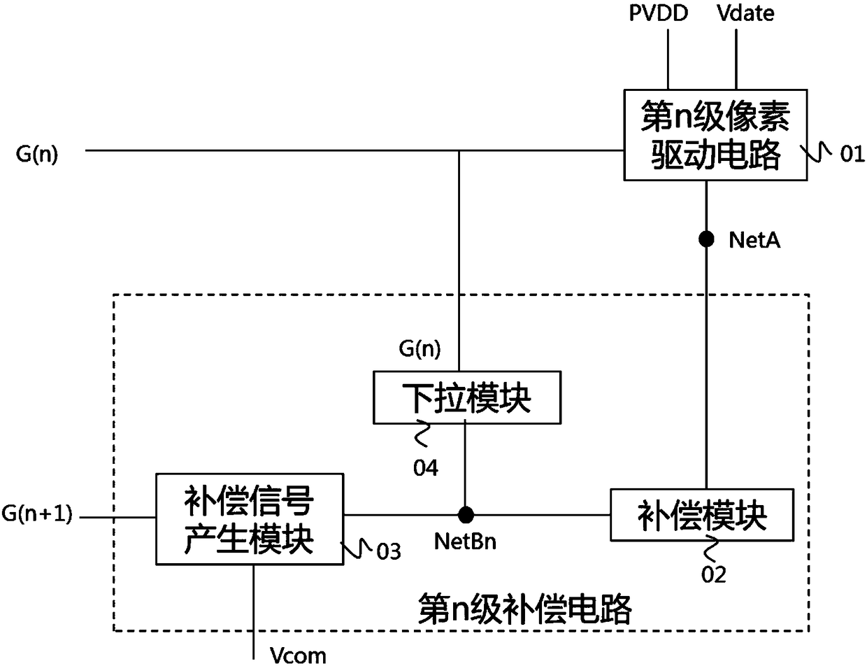
[0048] The organic light-emitting display in this embodiment includes N1 rows of scan lines and M columns of data lines (N1≥N>1, M>1 and N1 and M are integers), pixel areas defined by intersections of scan lines and data lines, and A driving circuit of an organic light emitting display composed of N-level driving circuit units. The nth (1≤n≤N) level driving circuit unit includes an nth level compensation circuit and a plurality of nth level pixel driving circuits.

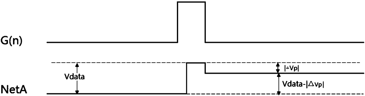
[0049] Figure 4 It shows the nth level compensation circuit and the kth region (1≤k≤N*M) pixel driving circuit belonging to one of the nth level pixel driving circuits, the kth region pixel driving circuit is located in the nth (1≤n≤N*M) pixel driving circuit ) in the mth (1≤m≤M) column pixel area, the kth area pixel driving circuit includes the kth area data node NetA(k), the nth level compensation circuit is connected to the kth area pixel driving circuit in the kth Zone data node NetA(k). The gate driving ci...


PUM


Abstract

The invention discloses a driving circuit of an organic light emitting display. The driving circuit comprises N stages of driving circuit units, wherein the nth (1<=n<=N, and n, N are integers)-stagedriving circuit unit comprises an nth-stage compensation circuit and a plurality of nth-stage pixel driving circuits; the nth-stage compensation circuit comprises a compensation signal generating module, a pull-down module and a plurality of compensation modules, and the compensation module and the nth-stage pixel driving circuits are connected to corresponding data nodes; when an nth-stage scanning signal is at high level, the nth-stage pixel driving circuits input actual data voltages into the data nodes; and when an (n+1)th-stage scanning signal is at high level, the compensation signal generating module is turned on and transmits a compensation signal to an nth-stage compensation node, and the compensation module compensates for the actual data voltage by means of the compensation signal. The driving circuit of the organic light emitting display compensates for data voltage jump caused by parasitic capacitance, and improves the precision of light emitting intensity of an organic light emitting diode.

Description

technical field [0001] The present invention relates to the field of organic light emitting display technology, in particular to a driving circuit of an organic light emitting display. Background technique [0002] The driving circuit of an organic light emitting display includes a plurality of pixel driving circuits arranged in a matrix. The existing structure of a pixel driving circuit is as follows: figure 1 As shown, it includes: a switching transistor T1, a driving transistor T2, a storage capacitor Cst, and an organic light emitting diode OLED (that is, 2T1C), and the nth-level pixel driving circuit scans the signal G(n), the data voltage Vdate, and the power supply in the n-level Driven by voltage PVDD. Among them, the driving transistor T2 is in a saturated state when it is working, so the working current I through the organic light emitting diode OLED Meet: I OLED =k*(Vgs 2 -Vth 2 ) 2 . Among them, k is the coefficient, Vgs 2 is the gate-source voltage diffe...

Claims


Application Information

Patent Timeline
Patent Type & Authority Applications(China)
IPC IPC(8): G09G3/3208
CPCG09G3/3208
Inventor 刘柱
Owner NANJING CEC PANDA LCD TECH
Why Eureka
Try Eureka